 ChipApex | Global Electronic Components Supplier

SEARCH
Search Product
Search Post
— IC芯片 | 连接器 | 传感器 | 被动器件 —
Search productSearch post
— IC芯片 | 连接器 | 传感器 | 被动器件 —
Consult the customer manager about the wholesale price.
consultation hotline:86-132-6715-2157
email:[email protected]
Contact the product manager for consultation. One-stop consultation is available.
Do you want a lower wholesale price? Please send us your inquiry and we will reply immediately.
ADCLK854BCPZ-REEL7 is listed in the Clock Buffers, Drivers range at ChipApex. The manufacturer field lists Analog Devices Inc.. Its product description is IC CLK BUF 2:12 1.2GHZ 48LFCSP. Review the specifications below when checking this part for your BOM.
The ADCLK854BCPZ-REEL7 is a low-power clock fanout buffer manufactured by Analog Devices Inc. It features two selectable differential inputs and up to 24 single-ended CMOS or 12 LVDS outputs, configurable via three control pins. The device operates on a 1.8 V ± 5% power supply (1.71 V to 1.89 V) within an industrial temperature range of -40°C to +85°C. It supports input frequencies up to 1.2 GHz for LVDS and 250 MHz for CMOS. Key electrical specifications include a maximum propagation delay of 2.7 ns for LVDS and 4.2 ns for CMOS, with integrated jitter of 54 fs rms (12 kHz to 20 MHz). The component is housed in a 48-pin LFCSP package.
Verify the specific ordering suffix against the manufacturer's current documentation to confirm packaging details. The REEL7 suffix indicates tape and reel packaging, which differs from tray packaging options available for other variants. Ensure compatibility with surface mount assembly processes suitable for the 48-LFCSP-VQ package dimensions.
Select this component when a low-jitter fanout buffer is required for high-speed digital interfaces. The choice between LVDS and CMOS outputs depends on the receiver requirements and board layout constraints. Consider the 1.8 V supply voltage requirement and ensure adequate decoupling capacitance near the VS pins to maintain signal integrity and minimize phase noise.
This part belongs to the ADCLK854 series of clock buffers. It is distinct from higher-frequency models like the ADCLK954, which supports up to 4.8 GHz. The ADCLK854 is optimized for applications requiring flexible logic level conversion and low power dissipation rather than extreme frequency multiplication or generation capabilities.
Direct pin-compatible replacements are not explicitly listed in the provided documentation. Designers should evaluate alternative Analog Devices clock buffers such as the ADCLK853 or ADCLK855, ensuring that input/output configurations, supply voltages, and thermal performance meet the original design specifications.
The outputs are grouped into three banks of four. Control pins CTRL_A, CTRL_B, and CTRL_C determine whether each bank operates as LVDS or CMOS. A logic low selects LVDS, while a logic high selects CMOS.
The SLEEP pin enables a power-down mode. When pulled high, it places the outputs in a high-Z state and powers down the internal circuitry, except for the internal bandgap reference.
Yes, single-ended inputs can be accommodated by AC or DC coupling to one side of the differential input pair, while the complementary input is bypassed to ground with a capacitor.
Explore related parts through Clock/Timing, Integrated Circuits (ICs), all product categories, ChipApex homepage.
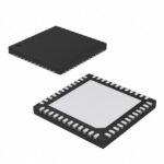 ADCLK854BCPZ-REEL7

The activity of extra discounts on wholesale prices is in full swing…
Please fill in your contact information and we will send you the latest wholesale price list.





