 ChipApex | Global Electronic Components Supplier
SEARCH
Search Product
Search Post
— IC芯片 | 连接器 | 传感器 | 被动器件 —
Search productSearch post
— IC芯片 | 连接器 | 传感器 | 被动器件 —
Consult the customer manager about the wholesale price.
consultation hotline:86-132-6715-2157
email:[email protected]
Contact the product manager for consultation. One-stop consultation is available.
Do you want a lower wholesale price? Please send us your inquiry and we will reply immediately.
The ADD8504WRUZ is a four-channel LCD gamma reference buffer designed for line inversion panels. It operates on a single supply voltage ranging from 3.3 V to 6.5 V with a typical supply current of 3.8 mA. The device features rail-to-rail input and output capabilities, ensuring compatibility with various logic levels. Key electrical specifications include a maximum offset voltage of 20 mV, a slew rate of 7.0 V/μs, and an output short-circuit current capability up to 380 mA. It is housed in a 16-lead Pb-free TSSOP package and functions reliably within a temperature range of −40°C to +105°C.
Verify the specific ordering suffix (e.g., REEL7) against the manufacturer's official documentation to confirm packaging type and quantity. Ensure the component meets RoHS compliance requirements if mandated by your design standards. Cross-reference the thermal resistance values provided in the datasheet with your PCB layout constraints to guarantee proper heat dissipation during operation.
Select this component when designing displays requiring precise gamma correction buffers with high current drive capabilities. The four-channel configuration suits applications needing independent control over multiple column driver inputs. Consider the wide operating temperature range and automotive qualification options if the deployment environment demands extended reliability or specific industry certifications.
This part belongs to the ADD850x family of LCD gamma buffers, which also includes five-channel (ADD8505) and six-channel (ADD8506) variants. These devices share similar architectural features but differ in pin counts and channel availability. The ADD8504 specifically utilizes a 16-lead TSSOP package, making it suitable for space-constrained designs compared to its higher-channel counterparts.
The ADD8505WRUZ and ADD8506WRUZ are direct functional equivalents within the same family, offering additional channels. Designers must verify pinout compatibility and software configuration changes required for the extra inputs and outputs before substituting these parts.
Each buffer channel has dedicated INA and INB pins. Applying a Logic High to the A/B select input connects the channel to the INA input, while a Logic Low connects it to the INB input, allowing dynamic switching between two pre-set gamma voltage curves.
No. The outputs are designed to drive both resistive and capacitive loads directly. Using series resistors is discouraged as it may degrade display performance; the buffers are stable with loads as low as 1 nF.
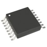 ADD8504WRUZ
The activity of extra discounts on wholesale prices is in full swing…
Please fill in your contact information and we will send you the latest wholesale price list.





