 ChipApex | Global Electronic Components Supplier
ADF4112BCPZ-RL7
Search Product
Search Post
— IC芯片 | 连接器 | 传感器 | 被动器件 —
Search productSearch post
— IC芯片 | 连接器 | 传感器 | 被动器件 —
Consult the customer manager about the wholesale price.
consultation hotline:86-132-6715-2157
email:[email protected]
Contact the product manager for consultation. One-stop consultation is available.
Do you want a lower wholesale price? Please send us your inquiry and we will reply immediately.
The ADF4112BCPZ-RL7 is an Integer-N RF PLL frequency synthesizer from Analog Devices, designed for local oscillator implementation in wireless systems. It operates with a maximum RF input frequency of 3.0 GHz and supports power supplies ranging from 2.7 V to 5.5 V. The device features a low-noise digital phase-frequency detector, a precision charge pump, and programmable dual-modulus prescalers (8/9, 16/17, 32/33, 64/65). It includes separate analog/digital supplies and a dedicated charge pump supply (VP) to extend tuning voltage capabilities. Typical operating current is 6.5 mA at 5 V, housed in a 20-pin LFCSP package.
Verify the B version industrial temperature rating (-40°C to +85°C) and LFCSP-20 packaging against design requirements. Confirm that the VP pin supply voltage does not exceed 6.0 V relative to ground. Ensure proper ESD handling procedures are followed during assembly due to the device's sensitivity.
Select this component when an RF input frequency up to 3.0 GHz is required. Ensure the external loop filter and VCO are compatible with the programmable charge pump range (up to 5 mA typ). Verify that the system can accommodate the separate VP supply if extended VCO tuning voltage is needed.
This part belongs to the ADF4110 family, which includes the ADF4110 (550 MHz), ADF4111 (1.2 GHz), and ADF4113 (4.0 GHz). All members share similar architectures and interfaces but differ in maximum RF input frequencies and associated performance specifications.
ADF4110BCPZ-RL7, ADF4111BCPZ-RL7, ADF4113BCPZ-RL7
The maximum allowable prescaler output frequency is 165 MHz at 3 V and 200 MHz at 5 V.
The charge pump current is set by connecting a resistor between the RSET pin and CPGND. With RSET = 4.7 kΩ, the typical maximum current is 5 mA.
Yes, AVDD and DVDD must be the same value (2.7 V to 5.5 V). However, the VP pin can be supplied separately up to 6.0 V to extend the tuning voltage range.
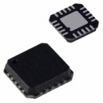 ADF4112BCPZ-RL7
The activity of extra discounts on wholesale prices is in full swing…
Please fill in your contact information and we will send you the latest wholesale price list.







