 ChipApex | Global Electronic Components Supplier
ADF4113HVBRUZ-RL
Search Product
Search Post
— IC芯片 | 连接器 | 传感器 | 被动器件 —
Search productSearch post
— IC芯片 | 连接器 | 传感器 | 被动器件 —
Consult the customer manager about the wholesale price.
consultation hotline:86-132-6715-2157
email:[email protected]
Contact the product manager for consultation. One-stop consultation is available.
Do you want a lower wholesale price? Please send us your inquiry and we will reply immediately.
The ADF4113HVBRUZ-RL is an integer-N frequency synthesizer featuring a high voltage charge pump capable of 15 V output. Designed for use with voltage-controlled oscillators (VCOs) requiring high tuning voltages, it operates directly with passive loop filters. The device integrates a low-noise digital phase frequency detector, programmable reference divider, dual-modulus prescaler, and A/B counters. It supports RF input frequencies from 200 MHz to 4.0 GHz and functions on power supplies ranging from 2.7 V to 5.5 V for logic/analog sections, while the charge pump supply (VP) ranges from 13.5 V to 16.5 V.
Verify the specific suffix RL against the manufacturer's current ordering guide to confirm packaging type and reel specifications. Ensure the VP supply pin is connected to a stable 13.5 V to 16.5 V source, as this differs from standard logic supplies. Confirm that the TSSOP-16 package thermal resistance requirements are met in the final PCB design.
Select the ADF4113HV when the target VCO requires a tuning voltage exceeding standard 5 V limits, eliminating the need for active loop filters. Choose the appropriate prescaler setting (e.g., 16/17 for 2 GHz inputs) to ensure the prescaler output remains below 200 MHz. Verify that the required charge pump current matches the available settings or external RSET value.
This component belongs to the ADF4113HV series, which is pin-compatible with the ADF4110, ADF4111, ADF4112, ADF4113, ADF4106, and ADF4002 synthesizers. It serves as the high-voltage variant within the broader ADF411x family, specifically engineered for applications where standard charge pumps cannot achieve the necessary VCO tuning range.
Direct pin-compatible replacements include the ADF4113, ADF4112, ADF4111, and ADF4110, though these lack the 15 V charge pump capability. For lower frequency applications, the ADF4002 may be considered. Ensure any substitute meets the specific high-voltage tuning requirements if present.
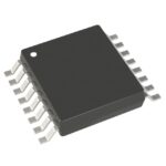 ADF4113HVBRUZ-RL
The activity of extra discounts on wholesale prices is in full swing…
Please fill in your contact information and we will send you the latest wholesale price list.





