 ChipApex | Global Electronic Components Supplier

SEARCH
Search Product
Search Post
— IC芯片 | 连接器 | 传感器 | 被动器件 —
Search productSearch post
— IC芯片 | 连接器 | 传感器 | 被动器件 —
Consult the customer manager about the wholesale price.
consultation hotline:86-132-6715-2157
email:[email protected]
Contact the product manager for consultation. One-stop consultation is available.
Do you want a lower wholesale price? Please send us your inquiry and we will reply immediately.
ADG509FBRN is listed in the Analog Switches, Multiplexers, Demultiplexers range at ChipApex. The manufacturer field lists Analog Devices Inc.. Its product description is IC SWITCH SP4T X 2 270OHM 16SOIC. Review the specifications below when checking this part for your BOM.
The ADG509FBRN is a CMOS analog multiplexer featuring four differential channels within a single 16-lead SOIC_N package. It provides fault protection by withstanding continuous overvoltage inputs from −40 V to +55 V, regardless of power supply status. The device utilizes a series n-channel, p-channel, n-channel MOSFET structure for signal and source protection. Key electrical parameters include a typical on-resistance (RON) of 270 Ω, maximum switching times of 230 ns (Ton) and 130 ns (Toff), and a maximum charge injection of 15 pC. It operates with dual supplies up to ±15 V or a single supply up to 15 V.
Verify the specific package variant, as the ADG509FBRN denotes the narrow-body SOIC option. Confirm RoHS compliance status if required, noting that suffixes like NZ indicate compliance. Ensure the design supports the industrial temperature range of -40°C to +85°C. Cross-reference pin configurations with the official datasheet to match logic control inputs A0, A1, and the Enable pin correctly.
Select this component for applications requiring differential signal switching with inherent overvoltage tolerance. The ADG509F differs from the ADG508F by offering four differential channels instead of eight single-ended channels. Consider the 270 Ω typical on-resistance and 15 pC charge injection limits for precision requirements. The break-before-make feature makes it suitable for multiplexers where signal overlap must be avoided.
The ADG509F belongs to the Analog Devices ADG508F/ADG509F family of fault-protected analog multiplexers. This series is designed for industrial and data acquisition environments where standard multiplexers might fail due to voltage transients or power loss events. The F-series variants generally offer improved performance characteristics compared to earlier generations, focusing on reliability and signal integrity under fault conditions.
Publicly confirmed substitutes include other ADI fault-protected multiplexers such as the ADG508F for single-channel applications. Verify pin compatibility and channel configuration (differential vs. single-ended) before substitution. Ensure the replacement part meets the same overvoltage withstand specifications (-40 V to +55 V) and operating temperature ranges.
When power supplies are off, the device's internal MOSFET structure ensures that inputs remain open-circuited with only nanoamperes of leakage current flowing, protecting both the multiplexer and the connected signal sources from damage.
This feature guarantees that the previous channel disconnects before the new channel connects, preventing momentary short circuits between different input signals during switching transitions.
Yes, the device can withstand continuous overvoltage inputs ranging from -40 V to +55 V, even if the power supplies are not present or are within the standard operational range.
Explore related parts through Interface, Integrated Circuits (ICs), all product categories, ChipApex homepage.
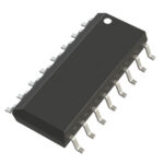 ADG509FBRN

The activity of extra discounts on wholesale prices is in full swing…
Please fill in your contact information and we will send you the latest wholesale price list.





