 ChipApex | Global Electronic Components Supplier

SEARCH
Search Product
Search Post
— IC芯片 | 连接器 | 传感器 | 被动器件 —
Search productSearch post
— IC芯片 | 连接器 | 传感器 | 被动器件 —
Consult the customer manager about the wholesale price.
consultation hotline:86-132-6715-2157
email:[email protected]
Contact the product manager for consultation. One-stop consultation is available.
Do you want a lower wholesale price? Please send us your inquiry and we will reply immediately.
ADG658YRUZ-REEL7 is listed in the Analog Switches, Multiplexers, Demultiplexers range at ChipApex. The manufacturer field lists Analog Devices Inc.. Its product description is IC MUX 8:1 75OHM 16TSSOP. Review the specifications below when checking this part for your BOM.
The ADG658YRUZ-REEL7 is an 8-channel analog multiplexer from Analog Devices, housed in a 16-lead TSSOP package. It operates on a single supply of 2 V to 12 V or dual supplies of ±2 V to ±6 V. The device features a maximum on-resistance of 75 Ω and a typical off-isolation of -90 dB at 1 MHz. Switching times include a maximum transition time of 115 ns and an enable turn-off time of 45 ns. It supports an automotive temperature range from -40°C to +125°C with low power consumption typically below 0.1 μW.
Verify the specific ordering suffix against official documentation to confirm packaging format and compliance status. The REEL7 suffix indicates tape and reel packaging. Confirm RoHS compliance and automotive qualification requirements if applicable to the target environment. Cross-reference the manufacturer part number with authorized distributor catalogs to ensure authenticity and traceability.
Select this component for designs requiring high channel density in a compact surface-mount package. Ensure the supply voltage range matches the system's available rails, as on-resistance varies with voltage. Verify that the digital logic levels are compatible with the input thresholds. Consider the thermal impedance of the TSSOP package for heat dissipation in dense layouts.
This part belongs to the ADG658/ADG659 family of low-voltage CMOS analog multiplexers. It is functionally similar to the ADG659 but provides eight single-ended channels instead of four differential pairs. The Y suffix denotes the extended automotive temperature grade. It serves as a drop-in replacement for legacy parts like the 74HC4051 in modern low-power designs.
Publicly confirmed pin-compatible upgrades include the ADG658YRU and ADG658YRUZ. Other family members like the ADG659 offer differential configurations. Legacy replacements such as the MAX4051 or 74HC4051 may require level shifting or voltage rail adjustments due to different electrical specifications.
The break-before-make time delay is typically 50 ns and has a minimum specification of 10 ns when switching between channels.
The EN pin is an active-low digital input. When driven high, all switches are disabled (OFF). When driven low, the address lines A0, A1, and A2 determine the active channel.
The charge injection is typically 2 pC when the source voltage is 0 V and the load capacitance is 1 nF.
Explore related parts through Interface, Integrated Circuits (ICs), all product categories, ChipApex homepage.
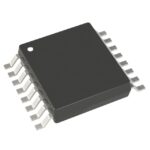 ADG658YRUZ-REEL7

The activity of extra discounts on wholesale prices is in full swing…
Please fill in your contact information and we will send you the latest wholesale price list.





