 ChipApex | Global Electronic Components Supplier

SEARCH
Search Product
Search Post
— IC芯片 | 连接器 | 传感器 | 被动器件 —
Search productSearch post
— IC芯片 | 连接器 | 传感器 | 被动器件 —
Consult the customer manager about the wholesale price.
consultation hotline:86-132-6715-2157
email:[email protected]
Contact the product manager for consultation. One-stop consultation is available.
Do you want a lower wholesale price? Please send us your inquiry and we will reply immediately.
The ADL5310ACP-WP is a dual logarithmic converter manufactured by Analog Devices Inc. It operates within a supply voltage range of 3 V to 12 V and draws a quiescent current of approximately 9.5 mA. The device provides two independent channels optimized for photodiode interfacing, supporting an input current range from 3 nA to 3 mA. It features a nominal slope of 10 mV/dB (200 mV/decade) with law conformance of 0.3 dB across the dynamic range. The component is housed in a space-efficient 24-lead 4 mm × 4 mm LFCSP package.
Verify the specific suffix 'WP' against official Analog Devices documentation to confirm its exact meaning regarding temperature grade or packaging configuration. Ensure compatibility with the standard 24-lead LFCSP footprint and validate that the selected variant meets the required operating temperature range of -40°C to +85°C for your application environment.
Select this component when designing systems requiring wide dynamic range optical power detection with minimal external calibration. The dual-channel architecture allows for simultaneous measurement of signal and reference currents, facilitating precise ratio operations. Consider the externally scalable slope and independently settable intercepts if your design demands customized transfer functions beyond the default specifications.
The ADL5310 serves as a low-cost alternative to higher-priced logarithmic amplifiers, offering enhanced dynamic range compared to predecessors like the AD8305. It is designed for fiber optic supervisory systems where determining optical power is critical. The integration of temperature compensation circuitry ensures stable performance across varying environmental conditions without requiring complex external components.
The ADL5310 is functionally equivalent to the dual AD8305 but provides an enhanced dynamic range of 120 dB. When substituting, verify that the replacement part supports the same 24-lead LFCSP package and maintains comparable quiescent current consumption to ensure thermal management requirements are met.
The nominal slope is 10 mV/dB (200 mV/decade). It can be modified using external resistors connected to the user-configurable output buffer amplifiers.
The VRDZ pin acts as an intercept shift reference input. Connecting it to VREF offsets the output voltage to position the intercept four decades below the reference current, enabling full dynamic range operation on a single supply.
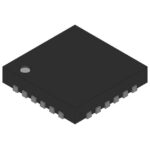 ADL5310ACP-WP

The activity of extra discounts on wholesale prices is in full swing…
Please fill in your contact information and we will send you the latest wholesale price list.






