 ChipApex | Global Electronic Components Supplier

SEARCH
Search Product
Search Post
— IC芯片 | 连接器 | 传感器 | 被动器件 —
Search productSearch post
— IC芯片 | 连接器 | 传感器 | 被动器件 —
Consult the customer manager about the wholesale price.
consultation hotline:86-132-6715-2157
email:[email protected]
Contact the product manager for consultation. One-stop consultation is available.
Do you want a lower wholesale price? Please send us your inquiry and we will reply immediately.
The ADL6316ACCZ-R7 is a transmit variable gain amplifier (VGA) manufactured by Analog Devices Inc. It operates within an RF frequency range of 500 MHz to 1000 MHz and is designed to interface RF DACs, transceivers, and SoCs with power amplifiers. The device utilizes a single 5 V supply and features a 38-terminal LGA package. Key electrical parameters include a typical power gain of 30.7 dB at 960 MHz, an output 1 dB compression point (OP1dB) of 24.7 dBm, and an output third-order intercept point (OIP3) of 41.1 dBm. The noise figure is typically 5.95 dB at the same frequency.
Verify that the specific ordering suffix matches the required reel quantity and tape specifications. Confirm the component meets RoHS compliance requirements for your assembly process. Ensure the PCB layout accommodates the exposed pad thermal requirements and differential input impedance matching as detailed in the datasheet.
Select this component when interfacing RF DACs to power amplifiers in the 500 MHz to 1000 MHz band. Consider the integrated balun and quadrature hybrids if minimizing external components is a priority. Evaluate the SPI programmability needs for dynamic gain adjustment versus fixed gain applications.
This part belongs to the ADL6316 Transmit VGA family from Analog Devices. It is specifically engineered for high dynamic range multicarrier transmitter designs. The device is fabricated using an advanced silicon germanium (SiGe) BiCMOS process to ensure high performance and linearity.
The ADL6317 is a related device in the same family but operates in the 1500 MHz to 3000 MHz frequency range. Verify frequency compatibility before substitution.
The VVA can be controlled internally via a 12-bit integrated DAC through the SPI interface or externally using an analog voltage applied to the VVA_ANALOG pin.
The TXEN pin serves as a hardware control for amplifier enable, DSA attenuation selection, and trim value selection, allowing for two predefined signal path modes without SPI latency.
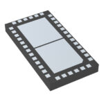 ADL6316ACCZ-R7

The activity of extra discounts on wholesale prices is in full swing…
Please fill in your contact information and we will send you the latest wholesale price list.





