 ChipApex | Global Electronic Components Supplier

SEARCH
Search Product
Search Post
— IC芯片 | 连接器 | 传感器 | 被动器件 —
Search productSearch post
— IC芯片 | 连接器 | 传感器 | 被动器件 —
Consult the customer manager about the wholesale price.
consultation hotline:86-132-6715-2157
email:[email protected]
Contact the product manager for consultation. One-stop consultation is available.
Do you want a lower wholesale price? Please send us your inquiry and we will reply immediately.
The ADL6316ACCZ is a transmit variable gain amplifier (VGA) manufactured by Analog Devices Inc. It operates within an RF frequency range of 500 MHz to 1000 MHz and interfaces RF DACs, transceivers, or SoCs to power amplifiers. The device features a 20.5 dB voltage variable attenuator (VVA) with on-chip DAC control and a 14 dB digital step attenuator (DSA) with 0.45 dB resolution. It utilizes two-stage high linearity amplifiers and includes an internal balun with bias tee. Key electrical parameters include a typical power gain of 30.7 dB at 960 MHz, an output 1 dB compression point (OP1dB) of 24.7 dBm, and an output third-order intercept point (OIP3) of 41.1 dBm. The noise figure is 5.95 dB at 960 MHz. It requires a single 5 V supply, drawing 435 mA in high performance mode, and is housed in a 38-terminal LGA package.
Verify the specific ordering suffix ACCZ corresponds to the standard LGA-38 package variant when sourcing. Confirm that the component meets RoHS compliance requirements for your assembly process. Ensure the PCB layout strictly follows the manufacturer's thermal resistance guidelines, particularly regarding the exposed pad connection to ground, to maintain specified junction temperatures and reliability under continuous operation.
Select this component for applications requiring precise gain control between 500 MHz and 1000 MHz. It is suitable for designs needing integrated impedance matching and conversion from differential to single-ended signals. Consider the 435 mA supply current and thermal dissipation characteristics during the initial design phase. Verify that the system architecture supports the required 4-wire SPI communication protocol for full functionality.
The ADL6316 belongs to a family of transmit VGAs designed for wireless infrastructure. It is part of a series that includes variants like the ADL6317, which covers higher frequencies up to 3000 MHz. These devices are built using silicon germanium (SiGe) BiCMOS technology to achieve high linearity and low noise figures essential for modern broadband communication standards.
The ADL6317 serves as a functional substitute for applications requiring similar VGA capabilities but operating in the 1500 MHz to 3000 MHz frequency range. Designers must account for the differences in frequency response and potentially different pinout or register configurations when migrating between these family members.
The device incorporates an internal balun that converts the 50 Ω differential RF input signals into a single-ended signal. This is followed by a quadrature hybrid to facilitate wideband performance and impedance matching.
The VVA attenuation can be controlled either internally via a 12-bit DAC through the SPI interface or externally by applying an analog voltage to the VVA_ANALOG pin.
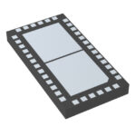 ADL6316ACCZ

The activity of extra discounts on wholesale prices is in full swing…
Please fill in your contact information and we will send you the latest wholesale price list.





