 ChipApex | Global Electronic Components Supplier
SEARCH
Search Product
Search Post
— IC芯片 | 连接器 | 传感器 | 被动器件 —
Search productSearch post
— IC芯片 | 连接器 | 传感器 | 被动器件 —
Consult the customer manager about the wholesale price.
consultation hotline:86-132-6715-2157
email:[email protected]
Contact the product manager for consultation. One-stop consultation is available.
Do you want a lower wholesale price? Please send us your inquiry and we will reply immediately.
The ADM203JNZ is a dual RS-232 line driver and receiver manufactured by Analog Devices Inc. It operates from a single +5 V power supply and integrates on-chip charge pump circuitry to generate ±10 V output swings, eliminating the need for external capacitors. The device features two drivers and two receivers, supporting transmission rates up to 120 kBaud. It complies with EIA-232-E and V.28 specifications and utilizes BiCMOS technology for low power consumption of approximately 10 mW. The component includes overvoltage protection on receiver inputs up to ±30 V and provides ESD protection exceeding 2 kV.
Verify the package designation matches the N-20 DIP configuration specified in the ordering guide. Confirm the suffix J indicates the commercial temperature range of 0°C to 70°C. Ensure the component source provides documentation confirming the absence of external charge pump capacitors, which distinguishes this model from the ADM202 variant.
Select this component when a single +5 V supply is available and PCB space for external capacitors is limited. The integrated charge pump simplifies layout compared to variants requiring discrete capacitors. Verify that the 120 kBaud rate meets system requirements and that the 20-pin DIP footprint aligns with the target board design constraints.
This part belongs to the ADM202/ADM203 family of high-speed CMOS RS-232 transceivers. It serves as an enhanced successor to the AD230–AD241 series, offering improved integration by embedding charge pump capacitors directly within the package. The JNZ suffix denotes the specific plastic DIP packaging and commercial operating temperature range defined by the manufacturer.
The ADM202JN is functionally similar but requires four external capacitors (C1+, C1-, C2+, C2-) for operation. Substitution requires adding these components to the schematic and verifying the 16-pin footprint compatibility against the existing 20-pin layout.
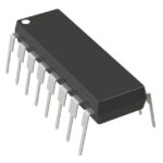 ADM203JNZ
The activity of extra discounts on wholesale prices is in full swing…
Please fill in your contact information and we will send you the latest wholesale price list.





