 ChipApex | Global Electronic Components Supplier
SEARCH
Search Product
Search Post
— IC芯片 | 连接器 | 传感器 | 被动器件 —
Search productSearch post
— IC芯片 | 连接器 | 传感器 | 被动器件 —
Consult the customer manager about the wholesale price.
consultation hotline:86-132-6715-2157
email:[email protected]
Contact the product manager for consultation. One-stop consultation is available.
Do you want a lower wholesale price? Please send us your inquiry and we will reply immediately.
The ADM239LJRZ is a CMOS RS-232 transceiver from Analog Devices, designed for EIA-232-E and V.28 interfaces. It features three drivers and five receivers in a 24-pin package. The device operates with a 5 V supply (VCC) and requires an external 7.5 V to 13.2 V supply (V+) for its internal charge pump, which generates the negative voltage rail. It supports data rates up to 120 kbps and includes a low-power shutdown mode drawing ≤1 µA. Key electrical parameters include ±9 V output swing, ±30 V receiver input protection, and Schmitt trigger inputs with 0.65 V hysteresis.
Verify the specific suffix 'JRZ' against the manufacturer's current ordering guide to confirm the exact package type and temperature grade. Confirm that the design accommodates the required external 7.5 V to 13.2 V supply voltage, as this part differs from standard single-supply variants.
Select the ADM239LJRZ when a system has an available positive supply between 7.5 V and 13.2 V but lacks a negative rail. This component reduces external component count compared to older generations while providing five receiver channels. Ensure the application utilizes the enable pin for bus sharing or power management.
This component belongs to the ADM2xxL family of line drivers and receivers. Unlike most members of this series that generate both positive and negative voltages from a single 5 V source, the ADM239L relies on an external positive supply to drive its internal charge pump. It serves as an enhanced upgrade to the legacy AD2xx series with improved power efficiency.
ADM231L
Unlike other parts in the ADM2xxL family, the ADM239L contains only a negative charge pump converter. It requires an external positive supply ranging from 7.5 V to 13.2 V to generate the necessary negative voltage for RS-232 signaling.
The EN pin is active low. When driven low, the receiver outputs are enabled. When driven high, the outputs enter a high-impedance state, allowing multiple devices to share a common data line without interference.
Each TTL/CMOS transmitter input has an internal 400 kΩ pull-up resistor to VCC. This ensures that unused inputs default to a high state, forcing the corresponding RS-232 outputs into a safe low state.
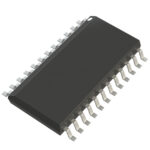 ADM239LJRZ
The activity of extra discounts on wholesale prices is in full swing…
Please fill in your contact information and we will send you the latest wholesale price list.





