 ChipApex | Global Electronic Components Supplier
ADN2806ACPZ
Search Product
Search Post
— IC芯片 | 连接器 | 传感器 | 被动器件 —
Search productSearch post
— IC芯片 | 连接器 | 传感器 | 被动器件 —
Consult the customer manager about the wholesale price.
consultation hotline:86-132-6715-2157
email:[email protected]
Contact the product manager for consultation. One-stop consultation is available.
Do you want a lower wholesale price? Please send us your inquiry and we will reply immediately.
The ADN2806ACPZ is a clock and data recovery (CDR) integrated circuit designed for SONET OC-12 applications. It automatically locks to 622 Mbps NRZ data without requiring an external reference clock or programming. The device features a patented delay- and phase-locked loop architecture that exceeds SONET jitter transfer, generation, and tolerance requirements. It operates on a single 3.3 V supply with typical power consumption of 359 mW. The unit provides differential LVDS outputs for recovered clock and data signals within a 32-lead LFCSP package.
Verify component authenticity through authorized Analog Devices distributors. Confirm RoHS compliance status as specified in the current datasheet revision. Check for moisture sensitivity level handling requirements during storage and assembly. Ensure ESD precautions are observed due to device sensitivity.
Select this component for fixed-rate 622 Mbps optical receiver designs requiring low power consumption. The device eliminates the need for external reference clocks, simplifying system design. Verify input signal compatibility with CML levels and ensure output buffering matches LVDS requirements. Consider thermal management for the 32-lead LFCSP package under maximum operating conditions.
The ADN2806 belongs to the ADN28xx family of clock and data recovery ICs from Analog Devices. It complements other devices like the ADN2804, which includes an integrated limiting amplifier. This specific part focuses on pure CDR functionality for cost-sensitive and power-constrained optical networking applications.
Direct replacements include the ADN2804ACPZ if an integrated limiting amplifier is required. For variable rate applications, consider the ADN2815ACPZ or ADN2817ACPZ. Verify pinout compatibility and electrical specifications before substitution.
No, the ADN2806 automatically locks to 622 Mbps data without an external reference clock. An optional reference clock can be used for acquisition aid via I2C configuration.
The SQUELCH pin disables clock and data outputs when driven high. It can be configured to squelch both outputs or selectively squelch data or clock outputs via I2C control.
The LOL pin asserts when the VCO frequency error exceeds 1000 ppm relative to the input data. It deasserts when the error is within 250 ppm. A static LOL mode is available via I2C to retain lock loss history.
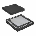 ADN2806ACPZ
The activity of extra discounts on wholesale prices is in full swing…
Please fill in your contact information and we will send you the latest wholesale price list.





