 ChipApex | Global Electronic Components Supplier
ADN2807ACPZ
Search Product
Search Post
— IC芯片 | 连接器 | 传感器 | 被动器件 —
Search productSearch post
— IC芯片 | 连接器 | 传感器 | 被动器件 —
Consult the customer manager about the wholesale price.
consultation hotline:86-132-6715-2157
email:[email protected]
Contact the product manager for consultation. One-stop consultation is available.
Do you want a lower wholesale price? Please send us your inquiry and we will reply immediately.
The ADN2807ACPZ is a clock and data recovery IC with an integrated limiting amplifier, designed for SONET/SDH applications. It supports OC-3 (155.52 Mbps), OC-12 (622.08 Mbps), and 15/14 FEC rates. The device features a patented dual-loop architecture combining delay-locked and phase-locked loops to minimize jitter peaking. It accepts CML differential inputs and provides CML differential outputs for recovered clock and retimed data. Operating on a single 3.0 V to 3.6 V supply, it consumes approximately 164 mA typical current in a 48-lead LFCSP package.
Verify the specific ordering suffix against the manufacturer's latest documentation to confirm packaging type and reel specifications. Confirm that the component meets RoHS compliance requirements for the intended deployment region. Check for any active product change notices that may affect pinout or electrical characteristics prior to finalizing procurement orders.
Select this component when designing receivers for OC-3 and OC-12 SONET/SDH interfaces requiring low jitter generation. Ensure the design accommodates the 48-lead LFCSP thermal requirements, utilizing the exposed pad for heat dissipation. Verify that the system reference clock frequency matches one of the supported options: 19.44 MHz, 38.88 MHz, 77.76 MHz, or 155.52 MHz.
The ADN2807 belongs to Analog Devices' specialized timing and clock support product line. It is part of a family of CDR devices tailored for optical communication standards. This specific model integrates the front-end limiting amplifier, reducing the need for external discrete components in fiber optic receiver designs compared to earlier generations.
Publicly confirmed substitute part numbers are not available in the provided documentation. Designers should consult the manufacturer's official replacement guide or contact technical support directly for qualified alternatives if this component becomes unavailable.
It uses a patented architecture combining a delay-locked loop for high-frequency jitter tracking and a phase-locked loop for low-frequency jitter filtering. This configuration eliminates the zero in the closed-loop transfer function, minimizing jitter peaking.
These pins allow for adjustable slice level offset of ±100 mV. This feature helps mitigate the effects of amplified spontaneous emission (ASE) noise in systems with optical amplifiers.
Yes, it includes an optional on-chip oscillator that can be used with an external crystal, selectable via the REFSEL pin.
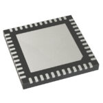 ADN2807ACPZ
The activity of extra discounts on wholesale prices is in full swing…
Please fill in your contact information and we will send you the latest wholesale price list.






