 ChipApex | Global Electronic Components Supplier
ADN2811ACPZ-CML
Search Product
Search Post
— IC芯片 | 连接器 | 传感器 | 被动器件 —
Search productSearch post
— IC芯片 | 连接器 | 传感器 | 被动器件 —
Consult the customer manager about the wholesale price.
consultation hotline:86-132-6715-2157
email:[email protected]
Contact the product manager for consultation. One-stop consultation is available.
Do you want a lower wholesale price? Please send us your inquiry and we will reply immediately.
The ADN2811ACPZ-CML is a clock and data recovery (CDR) integrated circuit designed for SONET OC-48 and SDH STM-16 applications, including 15/14 FEC digital wrapper rates. It operates at data rates of 2.48 Gbps and 2.66 Gbps with a single-supply voltage range of 3.0 V to 3.6 V. The device features CML differential inputs and outputs, a typical power consumption of 540 mW, and an operating temperature range from -40°C to +85°C. Packaged in a 48-lead LFCSP (7 mm × 7 mm), it integrates quantization, signal level detection, and jitter-compliant clock recovery.
Verify the specific suffix 'CML' against the manufacturer's official ordering guide to confirm interface compatibility. Confirm availability status through authorized distributors, as supply conditions may vary. Ensure compliance with RoHS directives and moisture sensitivity levels prior to procurement.
Select this component for designs requiring strict adherence to SONET/SDH jitter masks without external filtering. Ensure the PCB layout supports the 48-lead LFCSP package with adequate thermal dissipation for the exposed pad. Verify that the reference clock source matches one of the supported frequencies: 19.44 MHz, 38.88 MHz, 77.76 MHz, or 155.52 MHz.
The ADN2811 belongs to Analog Devices' specialized timing and clock recovery family, targeting high-speed optical networking infrastructure. It serves as a core receiver component for converting serial optical signals into retimed electrical data streams suitable for downstream processing in telecom systems.
Publicly confirmed substitute part numbers are not available in the provided documentation. Evaluate alternative CDR devices based on pin compatibility, jitter performance metrics, and package dimensions if direct replacement is required.
The ADN2811 utilizes a patented architecture combining a delay-locked loop and a phase-locked loop. This design places the zero required for frequency compensation in the feedback path rather than the closed-loop transfer function, effectively minimizing jitter peaking.
The device supports reference clocks of 19.44 MHz, 38.88 MHz, 77.76 MHz, and 155.52 MHz. The first three frequencies accept LVPECL, LVDS, LVCMOS, or LVTTL inputs, while 155.52 MHz is limited to LVPECL or LVDS.
No, the data rate is selected via the RATE input pin. Setting RATE to 0 configures the device for OC-48 (2.48 Gbps), while setting it to 1 configures it for OC-48 FEC (2.66 Gbps). A single reference clock frequency can be used for both modes.
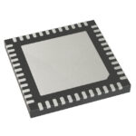 ADN2811ACPZ-CML
The activity of extra discounts on wholesale prices is in full swing…
Please fill in your contact information and we will send you the latest wholesale price list.





