 ChipApex | Global Electronic Components Supplier
ADN2812ACPZ
Search Product
Search Post
— IC芯片 | 连接器 | 传感器 | 被动器件 —
Search productSearch post
— IC芯片 | 连接器 | 传感器 | 被动器件 —
Consult the customer manager about the wholesale price.
consultation hotline:86-132-6715-2157
email:[email protected]
Contact the product manager for consultation. One-stop consultation is available.
Do you want a lower wholesale price? Please send us your inquiry and we will reply immediately.
The ADN2812ACPZ is a continuous-rate clock and data recovery (CDR) integrated circuit manufactured by Analog Devices Inc. It operates within a supply voltage range of 3 V to 3.6 V and supports serial data input rates from 12.3 Mb/s to 2.7 Gb/s. The device features a patented clock recovery architecture that automatically locks to all supported data rates without requiring an external reference clock or programming. It includes an integrated limiting amplifier with a typical quantizer sensitivity of 6 mV p-p and adjustable slice levels. The component meets SONET jitter requirements for transfer, generation, and tolerance. It is housed in a compact 5 mm × 5 mm 32-lead LFCSP package and operates across an ambient temperature range of −40°C to +85°C.
Verify the specific ordering suffix against the manufacturer's current documentation, as availability status may change. Confirm that the 32-LFCSP-WQ package dimensions match the target PCB footprint. Ensure that the I²C slave address configuration via Pin 19 aligns with the system bus design. Check for any recent revision history updates regarding electrical specifications or thermal characteristics before finalizing procurement.
Select this component for applications requiring high-speed clock recovery without the complexity of external reference clocks. The device is suitable for designs needing low jitter peaking due to its delay-locked loop architecture. Consider the 750 mW typical power dissipation when designing thermal management solutions for the LFCSP package. Verify that the input signal amplitude falls within the specified range for the integrated limiting amplifier to ensure proper quantization.
The ADN2812ACPZ belongs to the ADN2812 series of clock and data recovery ICs designed for optical communication receivers. It integrates the functions of quantization, signal level detection, and clock/data recovery into a single chip. This integration allows it to replace multiple discrete components, reducing board space and power consumption in fiber optic receiver modules operating at speeds up to 2.7 Gb/s.
Public confirmed substitute part numbers are not available in the provided source material.
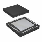 ADN2812ACPZ
The activity of extra discounts on wholesale prices is in full swing…
Please fill in your contact information and we will send you the latest wholesale price list.






