 ChipApex | Global Electronic Components Supplier
ADN2813ACPZ-RL7
Search Product
Search Post
— IC芯片 | 连接器 | 传感器 | 被动器件 —
Search productSearch post
— IC芯片 | 连接器 | 传感器 | 被动器件 —
Consult the customer manager about the wholesale price.
consultation hotline:86-132-6715-2157
email:[email protected]
Contact the product manager for consultation. One-stop consultation is available.
Do you want a lower wholesale price? Please send us your inquiry and we will reply immediately.
The ADN2813ACPZ-RL7 is a clock and data recovery IC from Analog Devices, designed for continuous serial data rates ranging from 10 Mb/s to 1.25 Gb/s. It integrates a limiting amplifier, quantizer, and PLL-based CDR circuit. The device operates on a single 3.0 V to 3.6 V supply with a typical current consumption of 139 mA at 1.25 Gb/s. It features LVDS outputs for recovered clock and data, an I2C interface for configuration, and supports SONET/SDH jitter requirements without an external reference clock.
Verify the specific ordering suffix '-RL7' against the manufacturer's official documentation to confirm reel packaging details. Confirm that the 'ACPZ' designation corresponds to the lead-free 32-LFCSP-WQ package variant. Ensure compatibility with the required 3.3 V single-supply operation and thermal management guidelines for the exposed pad.
Select this component for applications requiring automatic lock to data rates between 10 Mb/s and 1.25 Gb/s without external programming. Consider the 3.3 mV typical quantizer sensitivity and the need for an external TIA preamplifier if implementing a complete fiber optic receiver. Verify that the LVDS output swing and impedance match the downstream load requirements.
This part belongs to the ADN2813 series of clock and data recovery ICs. It is functionally similar to the ADN2812 but optimized for the 1.25 Gb/s rate. The device is often used in conjunction with PIN diodes and transimpedance amplifiers to form integrated optical receivers for high-speed serial communication systems.
Publicly confirmed substitute part numbers are not available in the provided source material. Evaluate alternatives based on pin compatibility, data rate support up to 1.25 Gb/s, and LVDS output specifications.
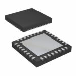 ADN2813ACPZ-RL7
The activity of extra discounts on wholesale prices is in full swing…
Please fill in your contact information and we will send you the latest wholesale price list.






