 ChipApex | Global Electronic Components Supplier
ADN2817ACPZ-RL7
Search Product
Search Post
— IC芯片 | 连接器 | 传感器 | 被动器件 —
Search productSearch post
— IC芯片 | 连接器 | 传感器 | 被动器件 —
Consult the customer manager about the wholesale price.
consultation hotline:86-132-6715-2157
email:[email protected]
Contact the product manager for consultation. One-stop consultation is available.
Do you want a lower wholesale price? Please send us your inquiry and we will reply immediately.
The ADN2817ACPZ-RL7 is a continuous rate clock and data recovery IC from Analog Devices, designed for serial data inputs ranging from 10 Mbps to 2.7 Gbps. It features an integrated limiting amplifier with 5 mV p-p sensitivity and adjustable slice levels. The device utilizes a proprietary dual-loop architecture to automatically lock to data rates without an external reference clock or programming. It operates on a single 3.0 V to 3.6 V supply, consuming 650 mW of power. Key specifications include jitter generation of 0.046 UI p-p at OC-48 and support for double data rate modes.
Verify the specific suffix RL7 indicates reel packaging when sourcing. Confirm availability status as distribution channels may list limited stock or end-of-life conditions. Ensure the LFCSP-32 package dimensions match the PCB footprint requirements during procurement planning.
Select this component for applications requiring high sensitivity (5 mV p-p) and adjustable slice levels via SLICEP/SLICEN pins. It is suitable for designs needing rate selectivity without a reference clock. Compare against the ADN2818 if higher input overdrive tolerance is required instead of maximum sensitivity.
This part belongs to the ADN2817/ADN2817 family of clock and data recovery ICs. It shares the same core architecture and pinout with the ADN2818, differing primarily in input stage sensitivity and limiting amplifier configuration. The ADN2817 is optimized for lower signal amplitude inputs compared to the ADN2818.
The ADN2818ACPZ-RL7 is a functional substitute within the same package, offering similar performance but with higher input sensitivity thresholds (200 mV p-p). Verify that the application does not require the specific 5 mV p-p sensitivity unique to the ADN2817.
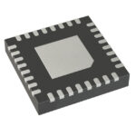 ADN2817ACPZ-RL7
The activity of extra discounts on wholesale prices is in full swing…
Please fill in your contact information and we will send you the latest wholesale price list.






