 ChipApex | Global Electronic Components Supplier
ADN2817ACPZ
Search Product
Search Post
— IC芯片 | 连接器 | 传感器 | 被动器件 —
Search productSearch post
— IC芯片 | 连接器 | 传感器 | 被动器件 —
Consult the customer manager about the wholesale price.
consultation hotline:86-132-6715-2157
email:[email protected]
Contact the product manager for consultation. One-stop consultation is available.
Do you want a lower wholesale price? Please send us your inquiry and we will reply immediately.
The ADN2817ACPZ is a continuous-rate clock and data recovery (CDR) integrated circuit manufactured by Analog Devices Inc. It supports serial data input rates from 10 Mbps to 2.7 Gbps without requiring an external reference clock or programming. The device features a proprietary dual-loop architecture, an integrated limiting amplifier with 5 mV p-p sensitivity, and adjustable slice levels. It operates on a single 3.3 V supply (3.0 V to 3.6 V range), consuming 650 mW of power. The component is housed in a compact 5 mm × 5 mm 32-lead LFCSP package and functions within an ambient temperature range of −40°C to +85°C.
Verify the specific ordering suffix against the manufacturer's current datasheet revision. Packaging variations such as tape-and-reel versus tray may exist for different part numbers within the same family. Confirm availability status directly with authorized distributors, as stock levels fluctuate. Ensure compliance with RoHS directives and moisture sensitivity level requirements during storage and handling.
Select the ADN2817ACPZ when high sensitivity (5 mV p-p) and adjustable slice levels are required, distinguishing it from the ADN2818 variant which lacks these features. Ensure the design accommodates the 3.3 V single-supply requirement and the 650 mW power dissipation. Verify that the 32-LFCSP package footprint matches the PCB layout guidelines provided in the datasheet, particularly regarding the exposed paddle connection to VEE.
The ADN2817ACPZ belongs to the ADN2817/ADN2818 series of clock and data recovery ICs designed for high-speed optical and electrical interfaces. It serves as a receiver function block for quantization, signal level detection, and clock/data recovery. The device is often paired with PIN diodes and TIA preamplifiers to form complete fiber optic receiver solutions. It shares the same package and core architecture with the ADN2818, differing primarily in input stage capabilities.
The ADN2818ACPZ is a pin-compatible alternative within the same series but lacks the integrated limiting amplifier and adjustable slice level features. It offers lower power consumption (600 mW) but requires higher input signal levels (200 mV p-p). No other direct cross-model replacements are documented in the provided source material.
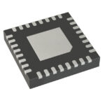 ADN2817ACPZ
The activity of extra discounts on wholesale prices is in full swing…
Please fill in your contact information and we will send you the latest wholesale price list.





