 ChipApex | Global Electronic Components Supplier
ADN2818ACPZ
Search Product
Search Post
— IC芯片 | 连接器 | 传感器 | 被动器件 —
Search productSearch post
— IC芯片 | 连接器 | 传感器 | 被动器件 —
Consult the customer manager about the wholesale price.
consultation hotline:86-132-6715-2157
email:[email protected]
Contact the product manager for consultation. One-stop consultation is available.
Do you want a lower wholesale price? Please send us your inquiry and we will reply immediately.
The ADN2818ACPZ is a continuous rate clock and data recovery IC designed for serial data inputs ranging from 10 Mbps to 2.7 Gbps. It operates on a single 3.0 V to 3.6 V supply, consuming a typical current of 180 mA (600 mW). The device features CML differential input and output interfaces within a 5 mm × 5 mm 32-lead LFCSP package. It automatically locks to data rates without external reference clocks or programming, exceeding ITU-T jitter specifications for SONET/SDH applications.
Verify the specific ADN2818 variant against the ADN2817, as the latter includes additional limiting amplifier and slice adjustment features not present in the ADN2818. Confirm that the 32-LFCSP exposed paddle is correctly connected to VEE during assembly to ensure proper thermal dissipation and electrical grounding.
Select the ADN2818 when high sensitivity or adjustable slice levels are not required, as these are exclusive to the ADN2817. Ensure the design accommodates the 180 mA typical supply current and verify that the 5 mm × 5 mm LFCSP footprint matches the PCB layout guidelines provided in the datasheet.
This component belongs to the ADN2817/ADN2818 family of clock and data recovery ICs manufactured by Analog Devices Inc. It shares the same core architecture and pinout with the ADN2817 but lacks the integrated limiting amplifier and programmable slice level controls found in the ADN2817 variant.
The ADN2817ACPZ is a compatible alternative within the same package if higher input sensitivity (5 mV p-p) or adjustable slice levels are needed. Other ADN281x derivatives like the ADN2812 or ADN2815 offer different maximum data rates or output formats and require careful interface verification.
No, the ADN2818 automatically locks to the incoming data rate without the need for an external reference clock or programming.
The differential input sensitivity is 200 mV p-p at a BER of 1 × 10⁻¹⁰ with ac-coupled PRBS 2²³−1 input.
The device includes a BERMON circuit that provides an estimate of the received bit error rate without interrupting the data, accessible via the I²C interface or an analog voltage output on the VBER pin.
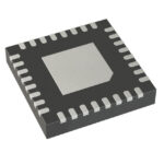 ADN2818ACPZ
The activity of extra discounts on wholesale prices is in full swing…
Please fill in your contact information and we will send you the latest wholesale price list.







