 ChipApex | Global Electronic Components Supplier
ADN2855ACPZ-R7
Search Product
Search Post
— IC芯片 | 连接器 | 传感器 | 被动器件 —
Search productSearch post
— IC芯片 | 连接器 | 传感器 | 被动器件 —
Consult the customer manager about the wholesale price.
consultation hotline:86-132-6715-2157
email:[email protected]
Contact the product manager for consultation. One-stop consultation is available.
Do you want a lower wholesale price? Please send us your inquiry and we will reply immediately.
The ADN2855ACPZ-R7 is a burst mode clock and data recovery IC designed for GPON, BPON, and GEPON optical line terminal receivers. It supports data rates of 155.52 Mbps, 622.08 Mbps, 1244.16 Mbps, and 1250.00 Mbps. The device features a patented dual-loop architecture with CML differential input and LVDS parallel or serial output. Operating on a single 3.3 V supply (3.0 V to 3.6 V), it consumes 670 mW in serial mode and 825 mW in deserializer mode. It acquires lock within 12 bits at higher speeds and operates from -40°C to +85°C in a 32-lead LFCSP package.
Verify the specific suffix R7 corresponds to the reel packaging configuration required for automated assembly. Confirm that the 32-LFCSP-VQ (5x5) package dimensions align with the target PCB footprint. Ensure the design supports the necessary I2C bus addressing and reference clock requirements specified in the datasheet.
Select this component for applications requiring burst-mode recovery in PON systems. Ensure the system provides a reference clock locked to the incoming data rate. Verify that the FPGA or ASIC interface supports the selected LVDS output mode (parallel nibble or serial). Check thermal constraints as the device dissipates up to 825 mW.
This part belongs to Analog Devices' specialized timing and clock recovery family. It is specifically engineered for downstream processing in passive optical networks where variable data rates and bursty traffic patterns are standard. The ADN2855 complements other OLT components by handling the critical task of retiming upstream bursts.
Public confirmed substitute part numbers are not available in the provided documentation. Evaluate pin-compatible alternatives only if they support identical burst mode acquisition times and LVDS output specifications.
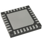 ADN2855ACPZ-R7
The activity of extra discounts on wholesale prices is in full swing…
Please fill in your contact information and we will send you the latest wholesale price list.






