ChipApex | Global Electronic Components Supplier
ADN2890ACP-RL7
Search Product
Search Post
— IC芯片 | 连接器 | 传感器 | 被动器件 —
Search productSearch post
— IC芯片 | 连接器 | 传感器 | 被动器件 —
Consult the customer manager about the wholesale price.
consultation hotline:86-132-6715-2157
email:[email protected]
Contact the product manager for consultation. One-stop consultation is available.
Do you want a lower wholesale price? Please send us your inquiry and we will reply immediately.
The ADN2890ACPZ-RL7 is a high-gain limiting amplifier designed for SONET, Gigabit Ethernet, and Fibre Channel optical receivers. It operates from a single 3.3 V supply with low power dissipation of 130 mW. The device supports data rates up to 2.7 Gb/s and can handle inputs up to 3.2 Gb/s for LX4 transceivers. Key electrical parameters include an input sensitivity of 3 mV p-p, 57 dB small signal gain, and CML outputs with 700 mV p-p differential swing. It features an integrated RSSI circuit compliant with SFF-8472 standards and a programmable LOS detector.
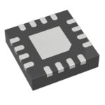
Verify the specific ordering suffix RL7 against the manufacturer's official documentation to confirm reel packaging specifications. Ensure compatibility with the required operating temperature range of -40°C to +85°C. Confirm that the 16-lead LFCSP package dimensions align with the target PCB layout constraints. Cross-reference the RoHS compliance status as indicated in the ordering guide.
Select this component when designing optical receivers requiring integrated signal monitoring and loss detection capabilities. The device eliminates the need for external RSSI circuitry due to its direct photodiode current measurement feature. Consider the 3 mm x 3 mm package size for space-constrained applications. Verify that the host system can accommodate the specified 3.3 V single-supply operation and associated decoupling requirements.
This part belongs to the ADN2890 series of limiting amplifiers manufactured by Analog Devices. It is specifically optimized for high-speed optical communication interfaces. The device integrates receiver front-end functions typically handled by multiple discrete components. It serves as a critical interface between the receive optical subassembly and the host digital logic.
The ADN2890ACPZ is listed as a compatible variant in the ordering guide. Verify pinout and functional equivalence before substitution. No other cross-model substitutes are documented in the provided datasheet.
The ADN2890 measures average received power by directly measuring the PIN photodiode current. The output is a current proportional to the average current supplied to the photodiode, which can be converted to a voltage using a resistor at the RSSI_OUT pin.
Driving the SQUELCH input to a logic high disables the limiting amplifier outputs. This pin can be connected to the LOS output to maintain static output voltages when the input signal drops below the programmed threshold.
 ADN2890ACP-RL7
The activity of extra discounts on wholesale prices is in full swing…
Please fill in your contact information and we will send you the latest wholesale price list.