 ChipApex | Global Electronic Components Supplier

SEARCH
Search Product
Search Post
— IC芯片 | 连接器 | 传感器 | 被动器件 —
Search productSearch post
— IC芯片 | 连接器 | 传感器 | 被动器件 —
Consult the customer manager about the wholesale price.
consultation hotline:86-132-6715-2157
email:[email protected]
Contact the product manager for consultation. One-stop consultation is available.
Do you want a lower wholesale price? Please send us your inquiry and we will reply immediately.
ADP1196ACBZ-02-R7 is listed in the Power Distribution Switches, Load Drivers range at ChipApex. The manufacturer field lists Analog Devices Inc.. Its product description is IC PWR SWITCH N-CHAN 1:1 6WLCSP. Review the specifications below when checking this part for your BOM.
The ADP1196ACBZ-02-R7 is a power distribution IC from Analog Devices, functioning as a high-side or low-side load switch. It supports an input voltage range of 0 V to 5.5 V and delivers up to 3 A output current. The device features an ultra-low on-resistance of 10 mOhms maximum and operates with a control supply (VB_EN) between 1.8 V and 5.5 V. It includes an internal charge pump for gate drive and offers a maximum turn-on time of 10 ms and turn-off time of 800 us. Packaged in a 6-pin WLCSP, it operates within a temperature range of -40°C to +85°C.
Verify component authenticity through authorized Analog Devices distributors or certified partners. Confirm the specific suffix matches project requirements, as variations may exist within the ADP1196 series. Ensure storage conditions comply with manufacturer guidelines for moisture-sensitive devices. Cross-reference datasheet revisions to confirm pinout and electrical characteristics align with design specifications before integration.
Select this component when zero-volt start-up capability is required for N-channel load switches. The integrated charge pump eliminates the need for external bootstrap components, simplifying board layout. Consider the 10 mOhm on-resistance for efficiency-critical designs. Verify that the 6-pin WLCSP package fits the available PCB footprint and thermal constraints.
This part belongs to the ADP1196 family of power switches designed for portable and industrial electronics. Unlike standard P-channel switches, it utilizes an N-channel MOSFET driven by an internal charge pump to achieve superior conduction losses. The family targets applications needing robust power management in space-constrained environments.
The device contains an internal charge pump that operates from either VIN or VB_EN, whichever is higher, allowing the N-channel MOSFET to conduct current even when the input voltage is close to zero.
The ADP1196ACBZ-02-R7 is designed to operate with an input voltage (VIN) ranging from 0 V to 5.5 V.
Explore related parts through Power Management (PMIC), Integrated Circuits (ICs), all product categories, ChipApex homepage.
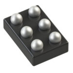 ADP1196ACBZ-02-R7

The activity of extra discounts on wholesale prices is in full swing…
Please fill in your contact information and we will send you the latest wholesale price list.





