 ChipApex | Global Electronic Components Supplier
ADP7159ACPZ-04-R7
Search Product
Search Post
— IC芯片 | 连接器 | 传感器 | 被动器件 —
Search productSearch post
— IC芯片 | 连接器 | 传感器 | 被动器件 —
Consult the customer manager about the wholesale price.
consultation hotline:86-132-6715-2157
email:[email protected]
Contact the product manager for consultation. One-stop consultation is available.
Do you want a lower wholesale price? Please send us your inquiry and we will reply immediately.
The ADP7159ACPZ-04-R7 is an adjustable linear regulator from Analog Devices, operating within a 2.3 V to 5.5 V input voltage range and delivering up to 2 A of load current. It provides an output voltage range of 1.2 V to 3.3 V with high power supply rejection ratio (PSRR) and ultralow noise characteristics. The device features a typical dropout voltage of 200 mV at full load and maintains initial accuracy of ±0.6%. It operates reliably across a temperature range of -40°C to +125°C and utilizes a 10-lead LFCSP package.
Verify the specific suffix '-04' corresponds to the required input/output voltage optimization for your design. Confirm the LFCSP-10 package footprint matches your PCB layout. Check for moisture sensitivity levels and reflow soldering profiles before assembly. Ensure the ordering part number includes the '-R7' tape and reel designation if automated placement is required.
Select this model when input voltages are between 3.8 V and 5.5 V and output requirements are near 3.3 V to minimize power dissipation. Consider the thermal resistance of the LFCSP package for high-current applications. Evaluate the need for external bypass capacitors on the BYP pin to further reduce low-frequency noise if necessary for sensitive analog circuits.
This component belongs to the ADP7159 family of RF linear regulators designed for noise-sensitive systems. It shares architectural similarities with the ADP7157 and ADP7158 but offers higher current capability. The family provides fixed and adjustable options to optimize efficiency based on specific voltage headroom requirements in communication infrastructure.
ADP7159ACPZ-04-R7
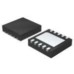 ADP7159ACPZ-04-R7
The activity of extra discounts on wholesale prices is in full swing…
Please fill in your contact information and we will send you the latest wholesale price list.




