 ChipApex | Global Electronic Components Supplier
ADR3530WBRMZ-R7
Search Product
Search Post
— IC芯片 | 连接器 | 传感器 | 被动器件 —
Search productSearch post
— IC芯片 | 连接器 | 传感器 | 被动器件 —
Consult the customer manager about the wholesale price.
consultation hotline:86-132-6715-2157
email:[email protected]
Contact the product manager for consultation. One-stop consultation is available.
Do you want a lower wholesale price? Please send us your inquiry and we will reply immediately.
The ADR3530WBRMZ-R7 is a micropower, high-precision CMOS voltage reference with a nominal output of 3.0 V. It features a maximum temperature coefficient of 5 ppm/°C and an initial output voltage error of ±0.1%. The device operates within an input voltage range of 3.2 V to 5.5 V and supports an operating temperature range from −40°C to +125°C. It provides an output current capacity of +10 mA source and −3 mA sink, with a maximum quiescent current of 100 μA. The component is qualified for automotive applications under AEC-Q100 standards.
Verify the specific grade (B grade) and suffix (-R7) against the manufacturer's ordering guide to ensure correct packaging and performance specifications. Confirm that the MSOP-8 package dimensions match the design footprint. Check for any recent product change notices regarding material or manufacturing site changes.
Select this component when a 3.0 V precision reference is required in an automotive environment. Ensure the input voltage remains within the 3.2 V to 5.5 V range to maintain specified regulation. Consider the thermal resistance and power dissipation limits if operating at high ambient temperatures or sourcing maximum load currents.
This part belongs to the ADR35xx series of micropower voltage references, which includes models with outputs of 2.5 V, 3.3 V, 4.096 V, and 5.0 V. All members of this family share similar architectural features, including CMOS construction, DigiTrim calibration, and automotive qualification, differing primarily in their nominal output voltage and corresponding input voltage requirements.
Other members of the ADR35xx family, such as ADR3525WBRMZ-R7, ADR3533WBRMZ-R7, ADR3540WBRMZ-R7, and ADR3550WBRMZ-R7, are pin-compatible alternatives offering different output voltages. Verify that the alternative voltage level meets the application requirements before substitution.
In a constant 50°C environment, the device exhibits a typical long-term drift of approximately 30 ppm after 1000 hours of continuous, unloaded operation.
When the ENABLE pin is pulled below 0.7 V, the device enters shutdown mode, reducing the quiescent current to a maximum of 5 μA.
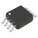 ADR3530WBRMZ-R7
The activity of extra discounts on wholesale prices is in full swing…
Please fill in your contact information and we will send you the latest wholesale price list.







