 ChipApex | Global Electronic Components Supplier
SEARCH
Search Product
Search Post
— IC芯片 | 连接器 | 传感器 | 被动器件 —
Search productSearch post
— IC芯片 | 连接器 | 传感器 | 被动器件 —
Consult the customer manager about the wholesale price.
consultation hotline:86-132-6715-2157
email:[email protected]
Contact the product manager for consultation. One-stop consultation is available.
Do you want a lower wholesale price? Please send us your inquiry and we will reply immediately.
The AFS1500-FGG256 is a Fusion FPGA from Microchip Technology, utilizing advanced 130-nm Flash-based CMOS technology. It features 1.5 million system gates and 38,400 configurable logic blocks (CLBs). The device operates with a supply voltage range of 1.42 V to 1.58 V, centered at 1.5 V. It supports a maximum system frequency of 350 MHz and includes an on-chip regulator for single 3.3 V operation. Packaged in a 256-ball FBGA with 1 mm pitch, it offers industrial temperature ratings from -40°C to +85°C.
Verify the specific suffix requirements for your application, as package variations exist. Confirm export compliance documentation needs, as this component may require additional files for international shipping. Check current manufacturing status, as some variants are transferred or obsolete. Ensure ESD handling procedures are followed due to moisture sensitivity classification.
Select this model when nonvolatile configuration and embedded processing are required in a single chip. Compare gate counts against other Fusion series devices if higher logic density is needed. Verify I/O count sufficiency for interface requirements. Consider thermal management solutions given the 350 MHz operational capability and FBGA package constraints.
This part belongs to the Microchip Fusion FPGA family, which combines Flash memory technology with programmable logic and optional embedded processors. It succeeds earlier Actel FPGA lines and integrates ARM cores for System-on-Programmable-Chip (SoPC) designs. The family emphasizes low power consumption and security features for harsh environments.
Direct pin-compatible replacements include the U1AFS1500-FGG256I and M1AFS1500-2FG256. Verify software compatibility and timing specifications before substitution. The P1AFS1500-FG256YES is listed but requires confirmation of functional equivalence regarding the embedded processor and I/O standards.
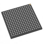 AFS1500-FGG256
The activity of extra discounts on wholesale prices is in full swing…
Please fill in your contact information and we will send you the latest wholesale price list.






