 ChipApex | Global Electronic Components Supplier
SEARCH
Search Product
Search Post
— IC芯片 | 连接器 | 传感器 | 被动器件 —
Search productSearch post
— IC芯片 | 连接器 | 传感器 | 被动器件 —
Consult the customer manager about the wholesale price.
consultation hotline:86-132-6715-2157
email:[email protected]
Contact the product manager for consultation. One-stop consultation is available.
Do you want a lower wholesale price? Please send us your inquiry and we will reply immediately.
The AFS250-2PQ208I is a Fusion mixed-signal Field Programmable Gate Array featuring 250,000 system gates and 6,144 tiles. It utilizes an advanced 130-nm flash-based CMOS process with seven metal layers. The device supports a maximum system performance of 350 MHz and includes 2 Mbits of embedded user flash memory alongside 1 Kbit of FlashROM. It integrates a 12-bit ADC capable of up to 600 Ksps sampling rate across 18 analog input channels. The component operates within a commercial temperature range of 0°C to +85°C and is housed in a PQFP-208 package.
Verify the specific speed grade suffix '2' corresponds to the required 25% faster timing specification relative to standard devices. Confirm the 'I' suffix indicates the intended industrial temperature rating if applicable, though datasheet tables list PQ208 availability primarily under commercial grades for this density. Ensure the ordering code matches the exact pinout and package dimensions defined for the PQFP-208 form factor.
Select this model when a single-chip solution integrating digital logic, analog sensing, and nonvolatile memory is required. The AFS250 offers sufficient gate density for moderate complexity designs while providing dedicated analog quads for signal conditioning. Consider the 350 MHz performance limit and 2 Mbit flash capacity against larger family members like the AFS600 if higher resource utilization is anticipated.
This component belongs to the Microsemi Fusion family of mixed-signal FPGAs, which combines flash-based programmable logic with analog peripherals. The AFS250 variant sits between the lower-density AFS090 and the higher-capacity AFS600 in terms of system gates and tile count. It shares architectural similarities with ARM Cortex-M1 enabled variants but lacks the integrated soft processor core.
Public confirmed substitute part numbers are not available in the provided documentation.


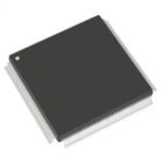 AFS250-2PQ208I
The activity of extra discounts on wholesale prices is in full swing…
Please fill in your contact information and we will send you the latest wholesale price list.



