 ChipApex | Global Electronic Components Supplier
SEARCH
Search Product
Search Post
— IC芯片 | 连接器 | 传感器 | 被动器件 —
Search productSearch post
— IC芯片 | 连接器 | 传感器 | 被动器件 —
Consult the customer manager about the wholesale price.
consultation hotline:86-132-6715-2157
email:[email protected]
Contact the product manager for consultation. One-stop consultation is available.
Do you want a lower wholesale price? Please send us your inquiry and we will reply immediately.
The AFS250-2PQG208 is a Fusion mixed-signal Field Programmable Gate Array (FPGA) manufactured by Microsemi Corporation. It features 250,000 system gates and 6,144 configurable logic blocks (tiles). The device operates on a single 3.3 V supply with an integrated 1.5 V regulator. Key specifications include 2 Mbits of embedded flash memory, 36 kbits of SRAM, and a 12-bit ADC supporting up to 18 analog input channels. It utilizes a PQFP-208 package with 114 maximum digital I/Os and supports speeds up to 350 MHz.
Verify the specific speed grade suffix required for the target frequency, as standard and faster grades exist. Confirm the temperature range designation matches the operational environment. Check for RoHS compliance status if environmental regulations apply. Ensure the ordering code includes the correct package type and security license options if cryptographic IP implementation is needed.
Select this device when a single-chip solution combining logic, memory, and analog conversion is required. Compare gate density against AFS090 or AFS600 variants based on logic resource needs. Consider the M1AFS250 variant if an embedded ARM Cortex-M1 processor is necessary for system management tasks alongside the FPGA fabric.
This component belongs to the Fusion family of mixed-signal FPGAs, which combines ProASIC3 flash architecture with analog peripherals. It is designed to replace costly discrete analog components and ASICs in system management and control applications. The family emphasizes low power consumption, high security, and rapid time-to-market through reprogrammability.
Direct pin-compatible replacements within the same package are limited due to the specific 250,000-gate density. The AFS090 offers lower density, while the AFS600 provides higher capacity but may require board redesign if pin counts differ significantly. Evaluate the M1AFS250 if soft processor integration is desired instead of pure logic functionality.
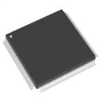 AFS250-2PQG208
The activity of extra discounts on wholesale prices is in full swing…
Please fill in your contact information and we will send you the latest wholesale price list.







