 ChipApex | Global Electronic Components Supplier
SEARCH
Search Product
Search Post
— IC芯片 | 连接器 | 传感器 | 被动器件 —
Search productSearch post
— IC芯片 | 连接器 | 传感器 | 被动器件 —
Consult the customer manager about the wholesale price.
consultation hotline:86-132-6715-2157
email:[email protected]
Contact the product manager for consultation. One-stop consultation is available.
Do you want a lower wholesale price? Please send us your inquiry and we will reply immediately.
The AGL015V2-QNG68I is a flash-based Field Programmable Gate Array (FPGA) from the Microsemi IGLOO family, utilizing a 130-nm process. It provides 15,000 system gates and 384 configurable logic blocks (CLBs). The device operates within a core voltage range of 1.14 V to 1.575 V, supporting both 1.2 V and 1.5 V systems. It features Flash*Freeze technology for ultra-low power consumption while retaining configuration data. The component is housed in a QN68 package with 68 terminals and supports an industrial temperature range from -40°C to +100°C.
Verify the specific ordering suffix 'I' confirms the industrial temperature grade (-40°C to +100°C). Confirm the 'V2' designation indicates support for the wide core voltage range (1.2 V to 1.5 V). Ensure the QN68 package matches the required footprint dimensions and pitch specifications for the target PCB layout.
Select this device for designs prioritizing nonvolatility and security over high-density logic. Note that the AGL015 lacks embedded RAM and PLL resources; verify if the application requires these features before choosing higher-density variants like the AGL030 or AGL060.
This part belongs to the IGLOO Low Power Flash FPGA family. It is architecturally compatible with other devices in the series but offers lower capacity. The datasheet notes that the AGL015 is not recommended for new designs, suggesting consideration of successor parts for long-term projects.
No direct public substitute part numbers are documented. Consider the AGL030 for increased logic capacity or the M1AGL series if ARM processor integration is required.
No, the AGL015 device does not support embedded SRAM or FIFO blocks.
The maximum operating junction temperature is +100°C for the Industrial grade variant.
Yes, the AGL015 supports ISP using on-chip 128-bit AES decryption via JTAG.


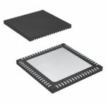 AGL015V2-QNG68I
The activity of extra discounts on wholesale prices is in full swing…
Please fill in your contact information and we will send you the latest wholesale price list.



