 ChipApex | Global Electronic Components Supplier
SEARCH
Search Product
Search Post
— IC芯片 | 连接器 | 传感器 | 被动器件 —
Search productSearch post
— IC芯片 | 连接器 | 传感器 | 被动器件 —
Consult the customer manager about the wholesale price.
consultation hotline:86-132-6715-2157
email:[email protected]
Contact the product manager for consultation. One-stop consultation is available.
Do you want a lower wholesale price? Please send us your inquiry and we will reply immediately.
The AGL400V5-FGG484 is a Field Programmable Gate Array from the IGLOO Low Power Flash FPGAs family, manufactured by Microsemi. It features 400,000 system gates and 9,216 VersaTiles (D-flip-flops). The device operates with a core voltage of 1.2 V to 1.5 V and supports up to 194 user I/Os in the FG484 package. It includes 54 kbits of True Dual-Port SRAM organized into twelve 4,608-bit blocks, one 1 kbit FlashROM, and six Clock Conditioning Circuits (CCC) with an integrated PLL. The maximum system performance is 250 MHz at 1.5 V or 160 MHz at 1.2 V. The component utilizes a 130-nm flash-based CMOS process and is housed in a 484-pin Fine Pitch Ball Grid Array (FBGA) package.
Verify the specific ordering suffix 'V5' indicates the correct version marking as per official documentation. Confirm that the FG484 package dimensions and pitch match the target PCB footprint requirements. Ensure the selected temperature grade aligns with the operational environment specifications defined in the datasheet.
Select this device when designs require nonvolatile configuration with low static power consumption. Consider the AGL400 density level if the design fits within 400,000 system gates and 9,216 VersaTiles. Verify that the required I/O standards are supported by the bank-selectable voltage options available on the chip.
This part belongs to the IGLOO Low Power Flash FPGAs family, which uses a 130-nm process. It is distinct from ARM-enabled M1IGLOO devices, as it does not support the Cortex-M1 soft processor. The V5 suffix denotes the specific revision of the IGLOO V2 device family.
Check for pin-compatible packages within the same IGLOO family such as FG256 or CS281 for different I/O counts. Higher density alternatives like AGL600 or AGL1000 may be considered if additional logic resources are needed.
Yes, the AGL400 device supports ISP using on-chip 128-bit Advanced Encryption Standard (AES) decryption via JTAG.
The typical power consumption in Flash*Freeze mode for the AGL400 device is 32 µW.
Yes, the Flash*Freeze pin can be routed internally or used as a regular I/O if Flash*Freeze mode usage is not planned.
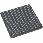 AGL400V5-FGG484
The activity of extra discounts on wholesale prices is in full swing…
Please fill in your contact information and we will send you the latest wholesale price list.






