ChipApex | Global Electronic Components Supplier
ALD1702APAL
Search Product
Search Post
— IC芯片 | 连接器 | 传感器 | 被动器件 —
Search productSearch post
— IC芯片 | 连接器 | 传感器 | 被动器件 —
Consult the customer manager about the wholesale price.
consultation hotline:86-132-6715-2157
email:[email protected]
Contact the product manager for consultation. One-stop consultation is available.
Do you want a lower wholesale price? Please send us your inquiry and we will reply immediately.
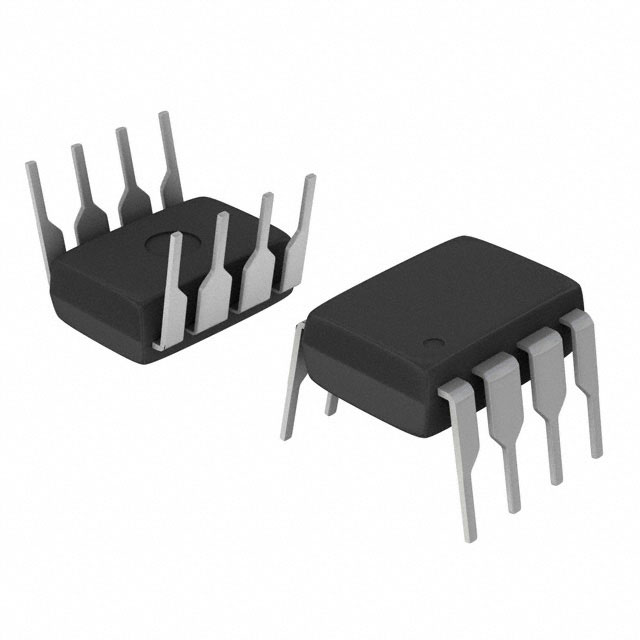
The ALD1702APAL is a monolithic precision operational amplifier manufactured using Advanced Linear Devices' ACMOS silicon gate CMOS process. It features rail-to-rail input and output voltage ranges, making it suitable for +5V single supply or ±5V dual supply systems. The device offers a unity gain bandwidth of 1.5MHz, a slew rate of 2.1V/µs, and extremely low input bias current of 1pA typical. It includes on-chip offset voltage trimming and operates within a temperature range of 0°C to +70°C in an 8-pin PDIP package.
Verify that the ordering suffix 'PAL' corresponds to the 8-pin Plastic DIP (PDIP) package variant as specified in the manufacturer's ordering information. Confirm that the component meets lead-free (RoHS) compliance requirements indicated by the 'L' suffix. Ensure the procurement specification aligns with the commercial operating temperature range of 0°C to +70°C rather than the extended industrial range available in other package options.
Select the ALD1702APAL when a precision CMOS op-amp with rail-to-rail capabilities is required for +5V or ±5V supply systems. The device is appropriate for mixed digital/analog circuits sharing a 5V power supply due to its compatibility with standard logic levels. Consider this part for applications demanding low power dissipation and high input impedance, such as sensor interfaces or charge integrators, where minimal loading of the signal source is critical.
The ALD1702APAL belongs to the ALD1702 family of rail-to-rail precision operational amplifiers from Advanced Linear Devices. This series is designed to offer a balanced trade-off of performance parameters for wide-range analog applications. The specific APAL designation identifies the plastic DIP packaging option within the broader product line that also includes SOIC and CERDIP variants.
The datasheet notes that the ALD1702A/ALD1702B/ALD1702/ALD1703 share the industry pin configuration of µA741 and ICL7611 types. Designers replacing legacy parts should verify that the new CMOS architecture supports the required load capacitance and input common-mode voltage switching behavior.
For unity gain buffers, the internal complementary input stage switching point occurs approximately 1.5V above the negative supply. Designers must account for potential input offset voltage variations if the common mode voltage approaches this threshold.
In a non-inverting unity gain connection, the device can typically drive up to 400pF of external load capacitance. In the inverting unity gain configuration, it can drive up to 800pF of load capacitance without stability problems.
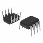 ALD1702APAL
The activity of extra discounts on wholesale prices is in full swing…
Please fill in your contact information and we will send you the latest wholesale price list.