ChipApex | Global Electronic Components Supplier
ALD2721EPBL
Search Product
Search Post
— IC芯片 | 连接器 | 传感器 | 被动器件 —
Search productSearch post
— IC芯片 | 连接器 | 传感器 | 被动器件 —
Consult the customer manager about the wholesale price.
consultation hotline:86-132-6715-2157
email:[email protected]
Contact the product manager for consultation. One-stop consultation is available.
Do you want a lower wholesale price? Please send us your inquiry and we will reply immediately.
The ALD2721EPBL is a dual micropower CMOS operational amplifier featuring integrated EPAD technology for user-programmable offset voltage trimming. It operates on a single supply of 2V to 10V or dual supplies of ±1V to ±5V. Key electrical parameters include a gain-bandwidth product of 0.7 MHz, a slew rate of 0.7 V/μs, and an input bias current of 10 pA maximum. The device offers rail-to-rail input and output capabilities, with an initial input offset voltage of 100 μV and a common-mode rejection ratio of 90 dB.
Verify the specific suffix 'BL' against the manufacturer's official ordering guide to confirm package type and temperature range, as standard listings may reference SOIC or CERDIP variants. Ensure compatibility with the ALD E100 programmer for EPAD configuration. Confirm RoHS compliance status for the specific revision. Check absolute maximum ratings regarding input voltage spikes relative to supply rails during integration.
Select this component when system-level calibration is required to compensate for external component tolerances and environmental drift. The EPAD feature allows trimming of total input offset voltage, including contributions from PSRR and CMRR, under actual operating conditions. Consider the 0.7 MHz bandwidth and 0.7 V/μs slew rate for moderate-speed precision applications requiring low power consumption.
The ALD2721E/ALD2721 series represents a dual-channel version of the monolithic precision CMOS operational amplifier family. It utilizes exclusive EPAD design to replace manual trimming procedures with automated, software-controlled programming. This architecture enables significant enhancement in total system performance by allowing individual amplifier offset adjustment within the circuit.
Public confirmed substitute part numbers are not available in the provided documentation. Verify pinout compatibility if considering alternative dual op-amps, specifically noting the four additional VE pins required for EPAD programming functionality.
Offset voltage is trimmed by applying incremental voltage pulses to the VE1 and VE2 pins using a standard EPAD Programmer. Increasing voltage on VE1 increases offset, while increasing voltage on VE2 decreases it. The programmed values are stored permanently in the device even after power-down.
The VE pins (VE1A, VE2A, VE1B, VE2B) are high-impedance terminals connected to internal offset bias circuits. They are used during programming mode to inject charge into the EPADs to adjust the input offset voltage. After programming, these pins must be left open.
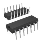 ALD2721EPBL
The activity of extra discounts on wholesale prices is in full swing…
Please fill in your contact information and we will send you the latest wholesale price list.