 ChipApex | Global Electronic Components Supplier

SEARCH
Search Product
Search Post
— IC芯片 | 连接器 | 传感器 | 被动器件 —
Search productSearch post
— IC芯片 | 连接器 | 传感器 | 被动器件 —
Consult the customer manager about the wholesale price.
consultation hotline:86-132-6715-2157
email:[email protected]
Contact the product manager for consultation. One-stop consultation is available.
Do you want a lower wholesale price? Please send us your inquiry and we will reply immediately.
ALD910030SALI is listed in the Special Purpose range at ChipApex. The manufacturer field lists Advanced Linear Devices Inc.. Its product description is DUAL SAB MOSFET ARRAY. Review the specifications below when checking this part for your BOM.
The ALD910030SALI is a dual-channel Supercapacitor Auto Balancing (SAB™) MOSFET array manufactured by Advanced Linear Devices, Inc. utilizing EPAD® technology. It provides precision voltage and current characteristics for balancing up to two series-connected supercapacitors. The device features a factory-trimmed gate threshold voltage of 3.00V at an output current of 1µA. Its effective resistance varies exponentially with input voltage, automatically regulating leakage currents to prevent overvoltages across the capacitor stack.
Verify the specific ordering suffix 'L' indicates lead-free compliance per RoHS standards. Confirm the 'I' suffix corresponds to the industrial operating temperature range of -40°C to +85°C. Ensure the SALI package designation matches the required 8-pin SOIC footprint for your design constraints.
Select this component when balancing exactly two series-connected supercapacitors. The ALD910030 offers a dual-channel configuration suitable for lower cell counts compared to the quad-channel ALD810030. Verify that the maximum drain-source voltage rating of 10.6V accommodates the individual supercapacitor voltage limits within the intended application stack.
This part belongs to the ALD9100xx family of SAB™ MOSFETs designed for automatic supercapacitor balancing. It utilizes production-proven EPAD® technology to address voltage and leakage-current issues in series stacks. The device integrates precision analog control directly into the MOSFET structure, eliminating the need for external discrete balancing circuits.
The ALD810030SALI serves as a functional substitute for applications requiring four-cell balancing instead of two. Both devices share identical core SAB™ technology and electrical characteristics but differ in channel count and package pinout.
It acts as an effective variable resistor connected across each supercapacitor. The resistance decreases exponentially as the voltage across the capacitor increases, shunting excess charge to maintain voltage equilibrium.
At 3.00V input, the device conducts 1µA. This precise point allows designers to set the maximum operating voltage limit for the supercapacitors, ensuring they do not exceed safe levels during charging.
No. When the input voltage drops below approximately 2.80V, the output current decreases significantly (to 0.01µA or less), resulting in essentially zero power dissipation.
Explore related parts through Transistors, Discrete Semiconductor Products, all product categories, ChipApex homepage.
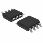 ALD910030SALI

The activity of extra discounts on wholesale prices is in full swing…
Please fill in your contact information and we will send you the latest wholesale price list.





