ChipApex | Global Electronic Components Supplier
AMP02FP
Search Product
Search Post
— IC芯片 | 连接器 | 传感器 | 被动器件 —
Search productSearch post
— IC芯片 | 连接器 | 传感器 | 被动器件 —
Consult the customer manager about the wholesale price.
consultation hotline:86-132-6715-2157
email:[email protected]
Contact the product manager for consultation. One-stop consultation is available.
Do you want a lower wholesale price? Please send us your inquiry and we will reply immediately.
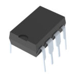
The AMP02FP is a high-accuracy instrumentation amplifier in an 8-lead plastic DIP package. It features laser-trimmed input offset voltage up to 200 µV and output offset voltage up to 8 mV at 25°C. Gain ranges from 1 to 10,000 via a single resistor. Bandwidth is 200 kHz at gain 1000 and 1.2 MHz at unity gain. Slew rate exceeds 4 V/µs. Input protection allows ±60 V overvoltage. Operating temperature range is –40°C to +85°C.
Verify the specific suffix FP corresponds to the 8-lead Plastic DIP package and the F grade specifications (200 µV max input offset). Confirm the operating temperature range matches the application requirements of –40°C to +85°C. Check datasheet revision E for updated electrical characteristics and outline dimensions before finalizing procurement.
Select this component when a precision instrumentation amplifier with integrated input overvoltage protection is required. The single-resistor gain setting simplifies circuit design compared to multi-resistor configurations. Ensure source impedance is balanced to minimize errors from input bias current. Consider the 200 µV maximum input offset voltage limit for high-gain applications where offset multiplication affects accuracy.
The AMP02 series represents Analog Devices' first precision instrumentation amplifier available in an 8-lead package. It utilizes a proprietary thin-film resistor process to achieve low gain temperature coefficients. The device employs a triple op amp topology with laser-trimmed input and output stages to maximize gain accuracy and common-mode rejection performance.
AMP02EP serves as a lower-offset alternative within the same package family. AMP02FS provides the same electrical characteristics in a 16-lead SOIC package. Verify pin compatibility and thermal resistance differences when substituting between package types.
The voltage gain is set by a single external resistor connected between pins RG1 and RG2. The gain equation is G = (50 kΩ / RG) + 1. No resistor is needed for unity gain.
In the 8-lead package, the Sense terminal is internally connected directly to the Output terminal. It completes the feedback path for the output stage.
Yes, the Reference pin can be used for offset correction or level shifting. However, connecting a reference source with non-zero resistance will reduce the common-mode rejection ratio.
 AMP02FP
The activity of extra discounts on wholesale prices is in full swing…
Please fill in your contact information and we will send you the latest wholesale price list.