 ChipApex | Global Electronic Components Supplier
SEARCH
Search Product
Search Post
— IC芯片 | 连接器 | 传感器 | 被动器件 —
Search productSearch post
— IC芯片 | 连接器 | 传感器 | 被动器件 —
Consult the customer manager about the wholesale price.
consultation hotline:86-132-6715-2157
email:[email protected]
Contact the product manager for consultation. One-stop consultation is available.
Do you want a lower wholesale price? Please send us your inquiry and we will reply immediately.
The AN17822A is a semiconductor device manufactured by Panasonic Semiconductor Singapore, housed in an FP-12S package. The component features a SiN chip surface passivation and utilizes a Fe group lead frame with Ag plating on the inner surface. Outer leads are solder plated using a 98Sn-2Bi alloy. Chip mounting employs Ag paste with thermalsonic bonding using Au wire. The mold material is epoxy, applied via a transfer mold process, with Cu group fins.
Verify the specific manufacturing revision against the document cover page history, noting changes to outer lead surface processes and chip mounting methods. Confirm compliance with lead-free specifications as amended in March 2005. Ensure the sourcing channel provides documentation matching the FMSC-PSDA-002-01 Rev 1 standard to guarantee alignment with the defined material composition and packaging details.
Select this component based on its specific FP-12S package dimensions and material constraints. The design requires compatibility with the defined Fe group lead frame and epoxy mold compound. Consider the thermalsonic bonding requirements and the specific 98Sn-2Bi outer lead plating when designing the assembly process. Verify that the application environment supports the defined Cu group fin structure and SiN passivation layer.
This specification defines the physical and material construction of the AN17822A semiconductor produced by Panasonic Semiconductor Singapore. It details the FP-12S package geometry, lead frame materials, and assembly techniques including wire bonding and molding. The document serves as the primary reference for the component's structural attributes rather than its electrical performance characteristics.
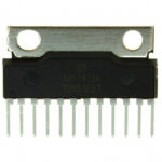 AN17822A
The activity of extra discounts on wholesale prices is in full swing…
Please fill in your contact information and we will send you the latest wholesale price list.






