 ChipApex | Global Electronic Components Supplier
SEARCH
Search Product
Search Post
— IC芯片 | 连接器 | 传感器 | 被动器件 —
Search productSearch post
— IC芯片 | 连接器 | 传感器 | 被动器件 —
Consult the customer manager about the wholesale price.
consultation hotline:86-132-6715-2157
email:[email protected]
Contact the product manager for consultation. One-stop consultation is available.
Do you want a lower wholesale price? Please send us your inquiry and we will reply immediately.
The AN5870K is a wide bandwidth analog switch IC designed for RGB and horizontal/vertical synchronizing signals. It features a built-in 75 Ω driver for video signals and utilizes a CMOS process for its sync. signal processing circuit to achieve high-speed operation. The device supports a broad range of monitors, from popular types to high-definition models. Key electrical parameters include a 300 MHz operation bandwidth, a 2-input 1-output DC switch configuration, and a built-in 6 dB amplifier for RGB signals (1.5 dB with 75 Ω termination). It also incorporates a built-in sync. separation circuit supporting sync. on green and power save functions.
Verify the specific package variant when ordering, as the datasheet notes a transition to a lead-free type (SDIP030-P-0400B) with updated dimensions. Confirm supply voltage requirements, as the IC operates with dual supplies: VCC1 at 5 V and VCC2 at 12 V. Ensure that peripheral components, particularly capacitors near pins 22 and 23, are placed close to the IC to prevent resonance phenomena around 400 MHz. Check for latch-up susceptibility on pins 20, 21, 28, and 30 during design validation.
Select the AN5870K for applications requiring wide bandwidth analog switching for RGB and sync signals up to 300 MHz. It is suitable for both standard and high-definition monitor designs. Consider the dual-supply architecture (5 V and 12 V) and the need for external 75 Ω termination resistors for optimal performance. Verify compatibility with sync-on-green signals if power-saving features are required. Ensure the chosen package version matches the mechanical constraints of the target PCB layout.
The AN5870K belongs to Panasonic's lineup of ICs for TV and monitor applications. It is specifically categorized as a wide bandwidth analog switch IC. The component is manufactured by Panasonic Electronic Components and is available in an SDIP package. It is designed to handle RGB signals and synchronization signals, making it a specialized solution for video signal routing and processing in display equipment.
Public confirmed substitute part numbers are not available in the provided documentation.
The C22 capacitor (0.01 µF) is used to correct resonance phenomena that occur at approximately 400 MHz between the B-out pin (pin 23) and the SW pin (pin 22). It should be placed as close to the IC as possible.
When the SW pin (pin 22) is low, it selects Input Pin 1 (pins 1, 5, 9, 13, 15). When the SW pin is high, it selects Input Pin 2 (pins 3, 7, 11, 14, 16).
The absolute maximum rating for VCC1 (pins 4, 8, 12) is 5.5 V, and for VCC2 (pins 28, 30) is 12.9 V.
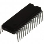 AN5870K
The activity of extra discounts on wholesale prices is in full swing…
Please fill in your contact information and we will send you the latest wholesale price list.





