 ChipApex | Global Electronic Components Supplier
SEARCH
Search Product
Search Post
— IC芯片 | 连接器 | 传感器 | 被动器件 —
Search productSearch post
— IC芯片 | 连接器 | 传感器 | 被动器件 —
Consult the customer manager about the wholesale price.
consultation hotline:86-132-6715-2157
email:[email protected]
Contact the product manager for consultation. One-stop consultation is available.
Do you want a lower wholesale price? Please send us your inquiry and we will reply immediately.
The AOZ5038QI is a high-efficiency synchronous buck power stage module from Alpha & Omega Semiconductor Inc. It integrates two asymmetrical MOSFETs and an integrated driver within a compact 5mm x 5mm QFN-31L package. The module supports a continuous output current of 50A with peak currents up to 60A. It operates with a power supply range of 4.5V to 25V and a driver supply range of 4.5V to 5.5V, enabling switching frequencies up to 2MHz.
Verify the specific suffix against official documentation, as ordering codes may indicate variations in packaging or environmental compliance. Confirm that the component meets RoHS standards if required by your design specifications. Ensure the supplier provides valid traceability data for quality assurance purposes during the acquisition process.
Select this module for applications requiring high efficiency at low duty cycles due to the optimized high-side MOSFET characteristics. Consider the thermal resistance values when designing heat dissipation strategies. Verify that the external controller logic aligns with the specified voltage thresholds for reliable PWM and FCCM signal interpretation.
This component belongs to the DrMOS power module family designed for synchronous buck conversion. It is intended to replace discrete MOSFET and driver solutions by integrating necessary components into a single package. The design aims to minimize parasitic inductance and EMI signatures through optimized pinout and layout considerations.
The AOZ5038QI is functionally compatible with Intel DrMOS specification IMVP8 (VRM13) in form fit and function. Designers should verify pinout compatibility and electrical parameters when substituting with other modules claiming similar standard adherence.
When the FCCM pin is held low, the low-side MOSFET enters diode emulation mode, allowing asynchronous operation. A high impedance state on this pin will shut down both MOSFETs.
The GL pin is brought out for diagnostic and manufacturing test purposes only. It is not directly connected to the internal gate pad, so it should not be connected in application circuits.
An adaptive timing circuit monitors the falling edge of the gate voltage and ensures dead time between switches. This prevents cross-conduction across the input bus even under transient conditions.
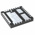 AOZ5038QI-05
The activity of extra discounts on wholesale prices is in full swing…
Please fill in your contact information and we will send you the latest wholesale price list.





