 ChipApex | Global Electronic Components Supplier
SEARCH
Search Product
Search Post
— IC芯片 | 连接器 | 传感器 | 被动器件 —
Search productSearch post
— IC芯片 | 连接器 | 传感器 | 被动器件 —
Consult the customer manager about the wholesale price.
consultation hotline:86-132-6715-2157
email:[email protected]
Contact the product manager for consultation. One-stop consultation is available.
Do you want a lower wholesale price? Please send us your inquiry and we will reply immediately.
The AOZ5507QI is a high-current, high-performance DrMOS power module from Alpha & Omega Semiconductor Inc. It integrates two asymmetrical MOSFETs and an internal driver for synchronous buck applications. The High-Side MOSFET features low capacitance and gate charge for fast switching, while the Low-Side MOSFET offers ultra-low ON resistance to minimize conduction loss. It operates with a 4.5V to 25V power supply range and a 4.5V to 5.5V driver supply. Peak current capabilities include up to 65A at 14V VIN and up to 80A with a 10us pulse. Switching frequency supports up to 2MHz.
Verify the exact part number against official manufacturer documentation before procurement. Confirm that the package type matches the required QFN3.5x4.5-22L footprint. Ensure environmental compliance requirements align with RoHS standards. Check for any specific handling precautions related to ESD sensitivity during assembly.
Select this component for applications requiring high efficiency in synchronous buck configurations. Consider the thermal performance characteristics when designing heat dissipation strategies. Evaluate the input voltage range compatibility with the system's power supply rails. Assess the switching frequency requirements against the module's operational limits.
This device belongs to the DrMOS power stage module family, combining power switches and drivers into a single package. It is designed to simplify PCB layout and reduce component count compared to discrete solutions. The integration allows for optimized performance in space-constrained designs.
Consult official manufacturer substitution guides for verified alternatives. Cross-reference electrical parameters such as current ratings and package dimensions carefully.
When the FCCM pin is high, the module operates in Continuous Conduction Mode (CCM). When low, it activates Discontinuous Conduction Mode (DCM) or diode emulation mode.
The Tri-State input allows the external controller to disable both High-Side and Low-Side MOSFETs by placing the PWM output in a high-impedance state.
An integrated bootstrap diode and an external capacitor connected between the BOOT and PHASE pins generate the necessary supply rail for the High-Side MOSFET gate driver.
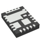 AOZ5507QI_2
The activity of extra discounts on wholesale prices is in full swing…
Please fill in your contact information and we will send you the latest wholesale price list.





