 ChipApex | Global Electronic Components Supplier
SEARCH
Search Product
Search Post
— IC芯片 | 连接器 | 传感器 | 被动器件 —
Search productSearch post
— IC芯片 | 连接器 | 传感器 | 被动器件 —
Consult the customer manager about the wholesale price.
consultation hotline:86-132-6715-2157
email:[email protected]
Contact the product manager for consultation. One-stop consultation is available.
Do you want a lower wholesale price? Please send us your inquiry and we will reply immediately.
The AOZ5517QI is a high-efficiency synchronous buck power stage module integrating two asymmetrical MOSFETs and an internal driver. It supports a 4.5V to 25V input range with a 60A continuous output current, peaking at 80A for 10ms pulses and 120A for 10µs pulses. The device operates up to 2MHz switching frequency using PWM or FCCM inputs compatible with 5V logic. Packaged in a compact 31-lead QFN (5mm x 5mm), it features integrated bootstrap diodes, UVLO protection, and optimized pinouts to minimize parasitic inductance.
Verify the specific suffix 'QI' against the manufacturer's datasheet to confirm the junction temperature range (-40°C to +150°C) and RoHS compliance status. Ensure ordering documentation matches the exact part number AOZ5517QI to avoid confusion with similar variants in the AOZ55xx series. Confirm package type is QFN5x5-31L.
Select this module for applications requiring high current density within a minimal footprint. The integrated design reduces component count compared to discrete solutions. Consider thermal management requirements carefully, as the exposed pads require adequate PCB copper area for heat dissipation. Verify that the controller supports the required PWM logic levels and Tri-State functionality.
This component belongs to the AOZ55xx DrMOS family from Alpha & Omega Semiconductor. These modules are designed for high-performance synchronous buck conversion. The AOZ5517QI specifically targets high-current applications where efficiency and switching speed are critical. It integrates power switches and drivers into a single package to reduce board space and improve reliability.
Direct substitutes include other AOZ55xx series parts such as AOZ5516QI_2 or AOZ5517NQI, provided voltage and current ratings match the application requirements. Cross-vendor replacements must be evaluated for pin compatibility, thermal performance, and electrical specifications.
When the FCCM pin is high, the module operates in Continuous Conduction Mode (CCM). When low, it enters Discontinuous Conduction Mode (DCM) or Diode Emulation Mode, allowing the Low-Side MOSFET to act as a synchronous rectifier only when current flows in one direction.
The Tri-State feature allows the High-Side and Low-Side MOSFETs to turn off completely when the PWM controller is in a high-impedance state. This prevents spurious triggering due to noise or glitches and ensures safe shutdown behavior.
The High-Side gate drive is powered by a bootstrap capacitor connected between the BOOT and PHASE pins. An internal bootstrap switch charges this capacitor during the Low-Side MOSFET conduction phase.
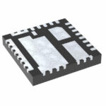 AOZ5517QI_2
The activity of extra discounts on wholesale prices is in full swing…
Please fill in your contact information and we will send you the latest wholesale price list.





