ChipApex | Global Electronic Components Supplier

SEARCH
Search Product
Search Post
— IC芯片 | 连接器 | 传感器 | 被动器件 —
Search productSearch post
— IC芯片 | 连接器 | 传感器 | 被动器件 —
Consult the customer manager about the wholesale price.
consultation hotline:86-132-6715-2157
email:[email protected]
Contact the product manager for consultation. One-stop consultation is available.
Do you want a lower wholesale price? Please send us your inquiry and we will reply immediately.
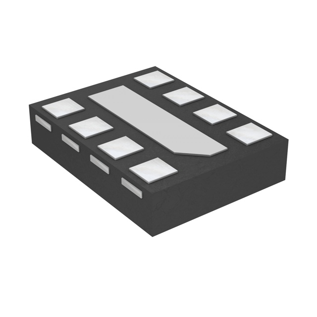
AP7345D-2818RH4-7 is listed in the Voltage Regulators - Linear, Low Drop Out (LDO) Regulators range at ChipApex. The manufacturer field lists Diodes Incorporated. Its product description is IC REG LIN 2.8V/1.8V X2DFN1612-8. Review the specifications below when checking this part for your BOM.
The AP7345D-2818RH4-7 is a dual low dropout regulator from Diodes Incorporated, packaged in an X2-DFN1612-8 footprint. It provides two independent positive fixed output channels: Channel 1 at 2.8V and Channel 2 at 1.8V. Each channel guarantees a continuous output current of 300mA with a wide input voltage range of 1.7V to 5.25V. The device features high ripple rejection of 75dB at 1kHz and low output noise of 60µVrms across the 10Hz to 100kHz bandwidth. Quiescent current is specified as low as 50µA per active channel, with standby current dropping to 1.0µA maximum when both enable pins are low.
Verify the specific ordering suffix RH4-7 confirms the X2-DFN1612-8 package and tape-and-reel packaging format. Ensure the part number matches the required 2.8V and 1.8V output combination. Confirm RoHS compliance status if restricted material usage is mandated by your design specifications.
Select this component when dual isolated rails are required within a minimal PCB area constraint. The 300mA per channel rating supports moderate load requirements without external pass transistors. Verify that the input voltage remains within the 1.7V to 5.25V window during all operating conditions to maintain regulation accuracy.
This device belongs to the AP7345D family of dual LDO regulators designed for portable electronics. It utilizes a CMOS process to achieve low quiescent current and small form factor. The series is engineered to replace discrete transistor solutions or single-channel regulators where space efficiency and multi-rail generation are critical design priorities.
AP7345D-2818FS4-7 (X1-DFN1612-8 package)
Setting an enable pin low activates standby mode for that channel, reducing quiescent current to a maximum of 1.0µA. Driving the pin high enables normal operation with a typical quiescent current of 50µA.
The datasheet recommends using ceramic capacitors with low ESR. A minimum 1µF input capacitor and appropriate output capacitors should be placed close to the VIN and VOUT pins respectively to ensure stability and transient response.
Explore related parts through Power Management (PMIC), Integrated Circuits (ICs), all product categories, ChipApex homepage.
 AP7345D-2818RH4-7

The activity of extra discounts on wholesale prices is in full swing…
Please fill in your contact information and we will send you the latest wholesale price list.