 ChipApex | Global Electronic Components Supplier
SEARCH
Search Product
Search Post
— IC芯片 | 连接器 | 传感器 | 被动器件 —
Search productSearch post
— IC芯片 | 连接器 | 传感器 | 被动器件 —
Consult the customer manager about the wholesale price.
consultation hotline:86-132-6715-2157
email:[email protected]
Contact the product manager for consultation. One-stop consultation is available.
Do you want a lower wholesale price? Please send us your inquiry and we will reply immediately.
The AS6500-FQFM is a four-channel time-to-digital converter (TDC) frontend device manufactured by ScioSense, housed in a QFN40 package. It provides single-shot RMS resolution of 20 ps, with options for 15 ps and 10 ps via high-resolution modes. The device supports a differential reference clock input ranging from 2 MHz to 12.5 MHz and features CMOS-level stop inputs. Data is transferred via an SPI interface with a maximum throughput of approximately 1.5 MSPS. Each channel includes a 16-stage FIFO buffer. Operating conditions range from -40°C to +125°C with a supply voltage of 3.3 V and power dissipation of 60 mW.
Verify the specific ordering code AS6500-FQFM against official ScioSense documentation to confirm the delivery form and reel quantity specifications. Ensure that the application environment remains within the recommended operating temperature and voltage limits defined in the datasheet to maintain performance integrity.
Select this component when high temporal resolution is required for optical ranging applications. Consider the available high-resolution modes if sub-20 ps accuracy is necessary, keeping in mind the associated reduction in peak conversion rate. Verify that the host microcontroller can support the required SPI clock frequency and data handling throughput.
The AS6500 is a derivative of the TDC-GPX2 series, specifically designed with CMOS inputs and serial SPI output capabilities. It maintains the core measurement performance of its predecessor while offering a simplified interface suitable for integration into compact electronic designs requiring precise time interval measurements.
The TDC-GPX2 serves as a functional equivalent within the same product family. Differences primarily involve input/output interface configurations and package types. Verify pin compatibility and register mapping before implementing any substitution in existing hardware designs.
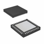 AS6500-FQFM
The activity of extra discounts on wholesale prices is in full swing…
Please fill in your contact information and we will send you the latest wholesale price list.





