 ChipApex | Global Electronic Components Supplier
SEARCH
Search Product
Search Post
— IC芯片 | 连接器 | 传感器 | 被动器件 —
Search productSearch post
— IC芯片 | 连接器 | 传感器 | 被动器件 —
Consult the customer manager about the wholesale price.
consultation hotline:86-132-6715-2157
email:[email protected]
Contact the product manager for consultation. One-stop consultation is available.
Do you want a lower wholesale price? Please send us your inquiry and we will reply immediately.
The ASNT1011A-PQA is a broadband digital serializer that multiplexes sixteen parallel LVDS data channels into a single high-speed serial CML stream. It operates over a data rate range from DC to 17 Gbps with a maximum power consumption of 660 mW at peak speed. The device utilizes a single +3.3 V supply and features a custom 100-pin QFN package (12mm x 12mm). It includes a full-rate clock output buffer and a divided-by-16 LVDS clock output with selectable phase shifts. The component supports industrial temperature operation from -25 °C to 125 °C junction temperature.
Verify the specific ordering suffix against the manufacturer's current documentation to ensure correct package type and pinout configuration. Confirm that the procurement source provides valid RoHS compliance certification per 2011/65/EU standards. Ensure handling procedures account for the custom QFN package requirements, particularly regarding thermal management without soldering the central heat slug unless explicitly connected to the positive supply plane.
Select this component when interfacing sixteen parallel LVDS sources to a serial link operating up to 17 Gbps. Ensure the system design accommodates the required external 50 Ohm series termination resistors for the CML outputs. Verify that the available clock source meets the frequency and swing requirements for the high-speed CML input buffer. Consider the industrial temperature range if the application environment exceeds standard commercial limits.
This device belongs to the ADSANTEC ASNT1011A family of broadband digital multiplexers. It serves as a high-performance serializer designed for applications demanding low jitter and precise clock-data alignment. The PQA suffix denotes the specific 100-pin QFN package variant, distinguishing it from other package options within the same functional family.
Publicly confirmed substitute part numbers are not available in the provided documentation. Evaluate alternative serializers based on matching data rates, interface compatibility, and package dimensions if direct replacement is required.
The phase of the divided-by-16 clock output can be modified in 90-degree increments using the CMOS control pins phs1 and phs2, which allow selection among 0°, 90°, 180°, and 270° phases.
By default, when the bitorder pin is set to logic low, the d00 channel is designated as the most significant bit (MSB) and serialized first.
Yes, the high-speed clock output buffer can be disabled to save power by setting the offcho control pin to logic high.
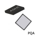 ASNT1011A-PQA
The activity of extra discounts on wholesale prices is in full swing…
Please fill in your contact information and we will send you the latest wholesale price list.





