 ChipApex | Global Electronic Components Supplier
SEARCH
Search Product
Search Post
— IC芯片 | 连接器 | 传感器 | 被动器件 —
Search productSearch post
— IC芯片 | 连接器 | 传感器 | 被动器件 —
Consult the customer manager about the wholesale price.
consultation hotline:86-132-6715-2157
email:[email protected]
Contact the product manager for consultation. One-stop consultation is available.
Do you want a lower wholesale price? Please send us your inquiry and we will reply immediately.
The ASNT2011-PQA is a broadband digital deserializer IC that functions as a 1-to-16 demultiplexer. It accepts serial CML input data at rates from DC to 17 Gbps and outputs 16 parallel LVDS channels operating at fbit/16, up to 1.125 Gbps. The device utilizes a single +3.3V supply with a maximum power consumption of 730 mW. It features internal 50 Ohm termination on high-speed inputs, a divide-by-16 clock path with selectable phase shifts, and operates within an industrial temperature range of -25°C to 125°C junction temperature.
Verify the specific ordering suffix PQA corresponds to the 100-pin QFN package variant when sourcing. Confirm RoHS compliance status per 2011/65/EU standards during acquisition. Ensure thermal management strategies account for the 730 mW power dissipation profile at maximum speeds. Validate that the supplier provides the official datasheet revision 2.4.2 or later for accurate pinout and electrical specifications.
Select this component when a single-ended or differential CML input must be converted into sixteen parallel LVDS signals. The device is suitable for applications requiring precise clock phase alignment via the CLK Proc block. Consider the 100-pin QFN footprint constraints and the requirement for a stable +3.3V power rail. This part is appropriate for industrial environments given its specified junction temperature range.
The ASNT2011 series includes variants such as the ASNT2011-KMA, which shares the same functional architecture but differs in package type. The PQA suffix specifically denotes the 100-pin QFN form factor. This device belongs to ADSANTEC's portfolio of high-speed digital multiplexers and demultiplexers designed for broadband communication infrastructure.
Publicly confirmed substitute part numbers are not available in the provided documentation. Evaluate the ASNT2011-KMA only if the package difference between QFN and CQFP can be accommodated by the design.
The phase of the cls output can be modified in 90-degree increments using the phs1 and phs2 CMOS control pins.
The LVDS output buffers support data rates up to 1.125 Gbps, corresponding to the fbit/16 division of the 17 Gbps input.
No, the Data IB and HS CIB buffers utilize on-chip single-ended termination of 50 Ohms to Vcc for each input line.
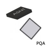 ASNT2011-PQA
The activity of extra discounts on wholesale prices is in full swing…
Please fill in your contact information and we will send you the latest wholesale price list.





