 ChipApex | Global Electronic Components Supplier
SEARCH
Search Product
Search Post
— IC芯片 | 连接器 | 传感器 | 被动器件 —
Search productSearch post
— IC芯片 | 连接器 | 传感器 | 被动器件 —
Consult the customer manager about the wholesale price.
consultation hotline:86-132-6715-2157
email:[email protected]
Contact the product manager for consultation. One-stop consultation is available.
Do you want a lower wholesale price? Please send us your inquiry and we will reply immediately.
The ASNT5107-KMC is a broadband tunable data and clock phase shifter fabricated in SiGe technology. It provides an adjustable delay range of 0 to 110 ps with stability of ±6 ps across a junction temperature range of 0°C to 125°C. The device supports data rates up to 32 Gbps and operates at frequencies up to 26 GHz when powered at maximum consumption, or 20 GHz at minimum power. It features fully differential CML input and output interfaces with internal 50 Ohm termination. Power supply options include a single +3.3V (with VEE grounded) or -3.3V (with VCC grounded). The part consumes between 630 mW and 1150 mW, with current draw adjustable from 190 mA to 350 mA via the ICRL control port.
Verify the specific revision level against the manufacturer's documentation prior to implementation. Confirm that the thermal management strategy accommodates the heat slug requirements for the custom CQFP package. Ensure that the power supply configuration matches the intended ground reference, as PCB layouts differ significantly between positive and negative supply modes.
Select this component when variable delay lines are required for high-speed signal integrity management. Consider the adjustable power consumption feature if thermal constraints are critical, noting that lower power reduces the maximum operational frequency to 20 GHz. Verify compatibility with the differential tuning port voltage ranges and ensure proper termination for the selected CML interface mode.
The ASNT5107-KMC belongs to the ASNT5107 family of phase shifters manufactured by Advanced Science And Novel Technology Company, Inc. It utilizes Silicon-Germanium (SiGe) fabrication technology to achieve high performance and reliability. The device is housed in a custom 24-pin CQFP package designed for efficient heat dissipation through a center heat slug on the underside of the package.
No public confirmed substitute part numbers are available in the provided documentation. Designers should consult ADSANTEC directly for potential alternative components within their portfolio or compatible third-party solutions.
The ICRL port adjusts the power consumption between minimum and maximum values. Higher voltages at this input increase power consumption, which in turn increases the operational speed of the part, allowing it to support higher data rates and frequencies.
If left unconnected, both the FBCRL (feedback gain) and EFCRL (internal peaking) ports default to an internal level of VCC-0.66V. This sets the respective currents to half their maximum values, placing the circuit in normal operating mode.
Yes, the I/Os support AC coupling. In AC-coupling mode, the input termination automatically provides the required common mode voltage. However, if using a positive supply configuration, all I/Os require AC termination when connected to devices with 50 Ohm termination to ground.
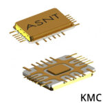 ASNT5107-KMC
The activity of extra discounts on wholesale prices is in full swing…
Please fill in your contact information and we will send you the latest wholesale price list.






