 ChipApex | Global Electronic Components Supplier
SEARCH
Search Product
Search Post
— IC芯片 | 连接器 | 传感器 | 被动器件 —
Search productSearch post
— IC芯片 | 连接器 | 传感器 | 被动器件 —
Consult the customer manager about the wholesale price.
consultation hotline:86-132-6715-2157
email:[email protected]
Contact the product manager for consultation. One-stop consultation is available.
Do you want a lower wholesale price? Please send us your inquiry and we will reply immediately.
The ASNT6104-KMM is a SiGe PAM4 decoder IC designed to convert one high-speed differential PAM4 input signal into two binary output data streams. It operates at a maximum data rate of 25 Gbaud with a corresponding clock frequency up to 25 GHz. The device features fully differential CML inputs and outputs, including a half-rate clock output synchronized with the data signals. Power consumption is specified at 2.4 W under typical conditions, supported by a single +3.3V or -3.3V supply configuration. Digital controls are managed via a 1.2V CMOS 3-wire interface, allowing adjustment of threshold levels and clock delay for optimal signal decoding.
Verify the specific revision level against the manufacturer's datasheet before integration, as pinout diagrams and electrical characteristics may have been corrected in updates such as Rev 1.2.2. Confirm that the PCB layout supports the required AC termination for I/Os when using positive supply configurations. Ensure thermal management strategies account for the 2.4 W power dissipation and solder the center heat slug to ground for effective heat removal.
Select this component when a dedicated silicon germanium solution is required for converting 25 Gbaud PAM4 signals to binary formats. Consider the requirement for a full-rate external clock input and the availability of a 3-wire interface for system control. Evaluate the need for adjustable threshold generation and clock delay alignment to accommodate varying signal integrity conditions in the target application environment.
Manufactured by Advanced Science And Novel Technology Company, Inc., the ASNT6104-KMM utilizes SiGe technology to achieve high-frequency performance. It is housed in a custom 44-pin CQFP package. The part number suffix indicates the package type and pin-out count, while the prefix identifies the circuit family and fabrication technology. The device complies with RoHS directives regarding restricted substances.
No public substitute part numbers are documented in the official datasheet. Designers should consult the manufacturer directly for potential alternative components or updated revisions if the current part becomes unavailable.
The HS Input Data and Clock buffers provide internal 50 Ohm termination to Vcc. The DC common mode voltage for the input signal must match the values specified in the Electrical Characteristics table; otherwise, external DC blocks are required.
The Voltage Threshold Generator (Vth GEN) creates two independent threshold voltage levels for the Comparator block. These levels are adjusted via two digital bytes in the SPI interface to define the decision boundaries for the PAM4 signal decoding.
Yes, the ASNT6104-KMM can operate with either a negative supply (Vcc = 0.0V and Vee = -3.3V) or a positive supply (Vcc = +3.3V and Vee = 0.0V). Different PCB layouts and AC termination requirements apply depending on the chosen configuration.
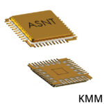 ASNT6104-KMM
The activity of extra discounts on wholesale prices is in full swing…
Please fill in your contact information and we will send you the latest wholesale price list.





