 ChipApex | Global Electronic Components Supplier
SEARCH
Search Product
Search Post
— IC芯片 | 连接器 | 传感器 | 被动器件 —
Search productSearch post
— IC芯片 | 连接器 | 传感器 | 被动器件 —
Consult the customer manager about the wholesale price.
consultation hotline:86-132-6715-2157
email:[email protected]
Contact the product manager for consultation. One-stop consultation is available.
Do you want a lower wholesale price? Please send us your inquiry and we will reply immediately.
The ASNT6104-PQB is a SiGe PAM4 decoder IC designed to convert one high-speed differential PAM4 input signal into two binary output data streams. It operates with a single +3.3V or -3.3V power supply and consumes 2.4W of power. The device supports data rates up to 17 Gbaud for PAM4 inputs and outputs, with a half-rate clock output at 8.5 GHz. Key electrical parameters include a typical junction temperature of 50°C (max 125°C), input swing of 0.05–0.6 V p-p, and output jitter of 3–5 ps p-p for data and 2–4 ps p-p for the clock. It features a 3-wire SPI interface for digital control and threshold adjustment.
Verify the specific package variant and revision level against the manufacturer's current documentation before ordering. Ensure that the power supply configuration matches the required I/O termination strategy, as positive and negative supply setups necessitate different PCB layouts and AC termination components for the I/O pins.
Select this component when a dedicated hardware solution is needed to decode PAM4 signals into binary formats without complex FPGA logic. Consider the thermal management requirements due to the 2.4W power consumption and ensure the host system can provide the necessary 1.2V CMOS logic levels for the 3-wire interface control.
The ASNT6104 series represents Advanced Science And Novel Technology Company's silicon-germanium (SiGe) integrated circuits for high-frequency signal processing. The PQB suffix denotes the standard 40-pin QFN package configuration. This family targets applications demanding low-jitter conversion and precise threshold control in high-speed serial links.
No publicly confirmed substitute part numbers are available in the official documentation. Direct replacement requires matching the SiGe technology node, PAM4 decoding functionality, and 40-pin QFN footprint.
The HS Input Data and Clock signals require a DC common mode voltage level of Vcc-0.8 to Vcc. If the source signal does not match this level, external DC blocks are required.
The delay block delivers a delayed version of the full-rate external clock to the decoder core. It allows phase shifting of the clock relative to the data to achieve optimal latching by the internal D-type flip-flops.
Yes, the Data Input Buffer (DIB) and External Clock Input Buffer (CIB) can accept single-ended signals. For single-ended operation, the unused differential pin must be terminated appropriately, such as applying a threshold voltage or DC termination.
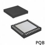 ASNT6104-PQB
The activity of extra discounts on wholesale prices is in full swing…
Please fill in your contact information and we will send you the latest wholesale price list.





