 ChipApex | Global Electronic Components Supplier

SEARCH
Search Product
Search Post
— IC芯片 | 连接器 | 传感器 | 被动器件 —
Search productSearch post
— IC芯片 | 连接器 | 传感器 | 被动器件 —
Consult the customer manager about the wholesale price.
consultation hotline:86-132-6715-2157
email:[email protected]
Contact the product manager for consultation. One-stop consultation is available.
Do you want a lower wholesale price? Please send us your inquiry and we will reply immediately.
The ASNT6119B-KMF is a SiGe-based advanced driver-amplifier (ADA) designed for high-speed data transmission applications. It features a built-in four-tap pre-emphasis generator controlled via a standard 3-wire serial interface. The device operates at data rates up to 33.5 Gbps with an average power consumption of 4.0W. It utilizes fully differential CML interfaces for data and clock signals, supporting both DC and AC coupling on inputs. The IC requires dual power supplies: a negative supply of -4.3V and a floating positive supply of +3.5V. It is housed in a custom 64-pin CQFP package with a center heat slug for thermal management.
Verify the specific revision level against the datasheet Rev.1.2.2 dated January 2020. Confirm that the system design accommodates the required dual power supply rails of -4.3V and +3.5V. Ensure the PCB layout supports the custom 64-pin CQFP package dimensions and provides adequate thermal dissipation for the center heat slug to maintain junction temperatures within specified limits.
Select this component when a fixed-rate driver is insufficient and programmable pre-emphasis is required to mitigate channel loss. The internal clock multiplier allows operation with lower input clock frequencies while maintaining high data throughput. Consider the analog control requirements for tap weights and duty cycle adjustments during the schematic design phase to ensure optimal signal performance across varying environmental conditions.
This device belongs to ADSANTEC's portfolio of high-speed silicon-germanium integrated circuits. It serves as a specialized solution for driving high-speed serial links where signal distortion must be actively compensated. The integration of digital control interfaces with analog tuning ports distinguishes it from standard buffer amplifiers, offering flexibility in system equalization strategies without external discrete components.
Public confirmed substitute part numbers are not available in the provided documentation. Designers should evaluate functional compatibility regarding pinout, power supply requirements, and interface protocols if considering alternative drivers from other manufacturers.
Pre-emphasis weights are adjusted using four external analog voltages (tune1 through tune4) for linear control, alongside digital signals that assign buffers to specific taps and determine their polarity.
The phadj pin serves a dual function: it activates the clock multiplier circuit and provides linear phase control to adjust the duty cycle of the multiplied-by-two clock signal.
Yes, applying a voltage below the switch-off threshold to the phadj pin disables the multiplication function, allowing the input clock to pass directly to the internal logic.
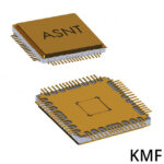 ASNT6119B-KMF

The activity of extra discounts on wholesale prices is in full swing…
Please fill in your contact information and we will send you the latest wholesale price list.





