 ChipApex | Global Electronic Components Supplier

SEARCH
Search Product
Search Post
— IC芯片 | 连接器 | 传感器 | 被动器件 —
Search productSearch post
— IC芯片 | 连接器 | 传感器 | 被动器件 —
Consult the customer manager about the wholesale price.
consultation hotline:86-132-6715-2157
email:[email protected]
Contact the product manager for consultation. One-stop consultation is available.
Do you want a lower wholesale price? Please send us your inquiry and we will reply immediately.
The ASNT6142-KHC is a broadband linear amplifier fabricated in SiGe technology, designed for receiver-side applications in high-speed communication systems. It operates from DC to 20 GHz with a differential gain of 25 dB at 10 GHz (vgc = vcc) and 10 dB at 10 GHz (vgc = vcc - 1.5V). The device features low jitter, limited temperature variation, and an output-referred 1dB compression point of 2.7 dBm single-ended at 20 GHz. Power consumption is 695 mW using a single +3.3V or -3.3V supply. It includes on-chip 50 Ohm termination, input offset adjustment, and a peak detector.
Verify the specific revision history and package details against the official ADSANTEC datasheet Rev. 1.1.2 before procurement. Confirm that the custom 24-pin CQFN footprint matches your PCB layout requirements. Ensure power supply configurations align with the recommended operating conditions for either positive or negative supply setups.
Select this component when designing high-speed links requiring wide bandwidth up to 20 GHz and precise gain control. Consider the SiGe fabrication for reliability and yield. Evaluate the thermal management needs due to the center heat slug requirement. Verify compatibility with CML logic levels and AC/DC coupling modes based on system interface requirements.
Manufactured by Advanced Science And Novel Technology Company, Inc., the ASNT6142-KHC belongs to a family of high-performance RF and microwave integrated circuits. It utilizes advanced SiGe technology to deliver robust performance in demanding environments. The part is housed in a custom CQFN package designed for efficient heat dissipation and compact integration.
No public confirmed substitute part numbers are available in the provided documentation.
Gain adjustment is performed through the external control port vgc. Differential gain is calculated by adding 6 dB to the single-ended gain values specified in the datasheet graph.
The device supports a single +3.3V supply (vcc = +3.3V, vee = 0V) or a single -3.3V supply (vcc = 0V, vee = -3.3V). Different PCB layouts are required for each configuration.
The pkdet pin provides a single-ended output voltage proportional to the input signal's amplitude, generated by the internal peak detector.
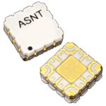 ASNT6142-KHC

The activity of extra discounts on wholesale prices is in full swing…
Please fill in your contact information and we will send you the latest wholesale price list.







