 ChipApex | Global Electronic Components Supplier
ASNT8051-PQB
Search Product
Search Post
— IC芯片 | 连接器 | 传感器 | 被动器件 —
Search productSearch post
— IC芯片 | 连接器 | 传感器 | 被动器件 —
Consult the customer manager about the wholesale price.
consultation hotline:86-132-6715-2157
email:[email protected]
Contact the product manager for consultation. One-stop consultation is available.
Do you want a lower wholesale price? Please send us your inquiry and we will reply immediately.
The ASNT8051-PQB is a programmable clock multiplication unit (CMU) fabricated in SiGe technology, featuring dual-range phase-locked loops (PLLs) with integrated voltage-controlled oscillators (VCOs). It operates on a single +3.3V supply with 570mW power consumption and supports junction temperatures from -40°C to 125°C. The device synthesizes high-speed clocks up to 17 GHz from lower-speed references. Key electrical parameters include a closed-loop SSB phase noise better than 98dB/Hz at 10MHz offset, peak-to-peak jitter of 6ps at 12.5GHz, and LVDS/CML/PECL input interface options. It is housed in a standard 40-pin QFN package.
Verify the specific ordering suffix against manufacturer documentation to confirm package type and pinout configuration. Ensure external loop filter components are selected according to the recommended schematic for target bandwidth and phase noise performance. Confirm thermal management requirements for the 40-pin QFN package given the 570mW power dissipation and operating temperature range.
Select the appropriate VCO range using the off12g control signal based on the required output frequency. Choose between full-rate and half-rate outputs via the offcho pin depending on downstream interface requirements. Ensure the reference clock source matches the supported input interface modes (LVDS, CML, or PECL) configured by the offecl pin. Verify that the external termination resistors match the specified impedance levels for optimal signal integrity.
The ASNT8051 series belongs to Advanced Science And Novel Technology Company's portfolio of high-performance RF clock generators. This specific model integrates both the PLL and VCO stages on a single SiGe die, reducing board space compared to discrete solutions. The -PQB suffix denotes the 40-pin QFN package variant, distinguishing it from other packaging options within the broader family.
Publicly confirmed substitute part numbers are not available in the provided documentation. When evaluating alternatives, ensure compatibility with the 40-pin QFN footprint, +3.3V supply voltage, and similar frequency ranges (up to 17 GHz output). Verify that replacement devices support the required CML/LVDS interfaces and offer comparable jitter specifications.
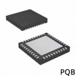 ASNT8051-PQB
The activity of extra discounts on wholesale prices is in full swing…
Please fill in your contact information and we will send you the latest wholesale price list.






