 ChipApex | Global Electronic Components Supplier
ASNT8160C-KMF
Search Product
Search Post
— IC芯片 | 连接器 | 传感器 | 被动器件 —
Search productSearch post
— IC芯片 | 连接器 | 传感器 | 被动器件 —
Consult the customer manager about the wholesale price.
consultation hotline:86-132-6715-2157
email:[email protected]
Contact the product manager for consultation. One-stop consultation is available.
Do you want a lower wholesale price? Please send us your inquiry and we will reply immediately.
The ASNT8160C-KMF is a programmable half-rate clock recovery (CR) circuit designed for high-speed data applications. It supports input data rates from 24.5 GHz to 32.0 GHz, corresponding to bit rates up to 64 Gb/s. The device utilizes three on-chip voltage-controlled oscillators (VCOs) to cover the operational frequency range. It accepts NRZ input data via CML differential interfaces and outputs a recovered half-rate clock signal also in CML format. Powered by a single +3.3V or -3.3V supply, the IC consumes up to 1.6W at maximum speed. It operates within an industrial junction temperature range of -25°C to 125°C.
Verify the specific VCO mode selection requirements based on the target input data rate using the vcos0 and vcos1 control pins. Ensure the external loop filter connected to pin ftr matches the design specifications for stable lock acquisition. Confirm the power supply configuration (positive or negative) as it dictates the required AC/DC termination strategy for all I/O connections.
Select this component when a half-rate clock output is required from a 24.5-32 GHz NRZ data stream. The device requires an external low-speed reference clock running at 1/32 the active VCO frequency. Designers must account for the 15°C/W thermal resistance and utilize the center heat slug for adequate heat dissipation. The package is a custom 64-pin CQFP which may require specialized PCB layout considerations.
The ASNT8160C-KMF belongs to the ASNT series of clock recovery circuits manufactured by Advanced Science And Novel Technology Company, Inc. It is distinct from demultiplexers like the ASNT2111-KMF as it focuses solely on clock recovery rather than data splitting. The 'KMF' suffix denotes the specific 64-pin CQFP package variant.
No direct public substitute part numbers are documented. Due to the proprietary nature of the VCO tuning and interface specifications, any replacement must be evaluated against the specific frequency ranges and electrical characteristics defined in the datasheet.
The desired working frequency is selected using the 2.5V CMOS control pins vcos0 and vcos1. Table 1 in the datasheet defines three modes covering different frequency bands up to 32.0 GHz.
The phshft pin is used to adjust the phase of the internal half-rate clock. It accepts a DC voltage ranging from vcc to vcc-1.0V to align the clock phase correctly with the incoming data signal.
Yes, the Data IB and HS CIB buffers can accept single-ended signals. For single-ended operation, a correct threshold voltage must be applied to the unused input pin.
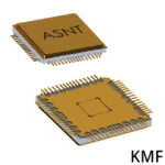 ASNT8160C-KMF
The activity of extra discounts on wholesale prices is in full swing…
Please fill in your contact information and we will send you the latest wholesale price list.






