 ChipApex | Global Electronic Components Supplier
ASNT8161-KMF
Search Product
Search Post
— IC芯片 | 连接器 | 传感器 | 被动器件 —
Search productSearch post
— IC芯片 | 连接器 | 传感器 | 被动器件 —
Consult the customer manager about the wholesale price.
consultation hotline:86-132-6715-2157
email:[email protected]
Contact the product manager for consultation. One-stop consultation is available.
Do you want a lower wholesale price? Please send us your inquiry and we will reply immediately.
The ASNT8161-KMF is a programmable half-rate clock recovery (CR) circuit designed for input data rates from 36 Gbps to 72 Gbps. It supports both NRZ and PAM4 data formats and utilizes six on-chip voltage-controlled oscillators (VCOs) to cover a wide frequency range. The device accepts CML or LVDS reference clocks and provides a half-rate CML clock output up to 36 GHz. Powered by a single +3.3V or -3.3V supply, it consumes 1.7W at maximum speed. Control is managed via a 3-wire SPI interface, allowing adjustment of VCO selection, charge pump current, and signal peaking.
Verify the specific package variant and revision level against the latest manufacturer datasheet before procurement. Confirm power supply configuration requirements, as the device supports both positive (+3.3V) and negative (-3.3V) supply polarities, which necessitates distinct PCB layouts. Ensure external loop filter components match the recommended schematic values for stable operation.
Select this component when a half-rate clock recovery solution is required for data rates between 36 Gbps and 72 Gbps. Consider the available VCO bands defined by the vcosel parameter to ensure the target frequency falls within the operational range. Evaluate the need for PAM4 support and input/output peaking adjustments, which are unique features of this IC compared to standard CR circuits.
The ASNT8161-KMF belongs to the ASNT series of clock recovery circuits manufactured by Advanced Science And Novel Technology Company, Inc. It is housed in a custom 64-pin CQFP package with a center heat slug for thermal management. The part number suffix 'KMF' indicates the specific package type and pinout configuration provided by the manufacturer.
No publicly confirmed substitute part numbers are available in the source documentation. Designers should evaluate compatibility based on pinout, electrical specifications, and package dimensions if considering alternative vendors.
The device supports both NRZ (Non-Return-to-Zero) and PAM4 (Pulse Amplitude Modulation 4-level) input data formats.
The desired working frequency is selected using the 3-bit digital control vcosel via the SPI interface, which chooses one of six on-chip VCO bands.
An off-chip passive filter must be connected to the ftr pin. The recommended schematic includes a 22nF capacitor, a 66 Ohm resistor, and a 390pF capacitor.
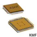 ASNT8161-KMF
The activity of extra discounts on wholesale prices is in full swing…
Please fill in your contact information and we will send you the latest wholesale price list.






